| May 15, 2014 |
X-rays, computer simulations reveal crystal growth
|
|
(Nanowerk News) Taking a step toward much-coveted flexible electronics, an international research team that figured out how to coat an organic material as a thin film – like spreading butter on toast – wanted a closer look at why their spreadable organic semiconductor grew like it did.
|
|
Enter Cornell scientists and the Cornell High Energy Synchrotron Source (CHESS), where a very tiny, extremely bright X-ray beam lit the way for high-speed movies showing how these organic molecules formed crystal lattices at the nanoscale. Understanding and tuning this process is key to advancing the technology from lab-only to mass production.
|
|
The visualization of the crystallization process is detailed in an April 16 Nature Communications online publication ("One-dimensional self-confinement promotes polymorph selection in large-area organic semiconductor thin films") and involves scientists from Stanford University, King Abdullah University of Science and Technology, and Cornell. The Cornell team included CHESS staff scientist Detlef Smilgies, who led the experiments on the D1 X-ray beamline at CHESS; and Paulette Clancy, professor of chemical and biomolecular engineering, who provided the key theoretical backbone to support the experimental findings.
|
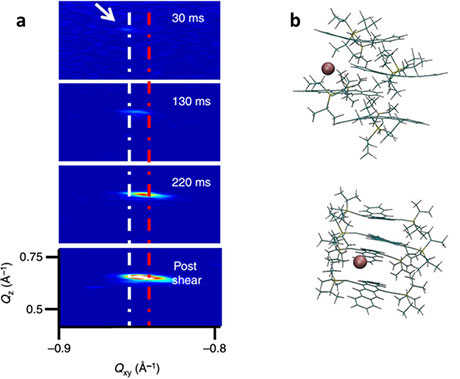 |
| Left: Evolution of the organic semiconductors' equilibrium structure (top) to the strained structure (bottom) in the light of CHESS X-rays. Right: Cornell researchers’ molecular simulations show that even a single solvent molecule (sphere) can significantly distort the molecular configuration of the surrounding organic semiconductor molecules (green).
|
|
Stanford engineers had previously described a method called solution shearing that applies a thin layer of organic semiconductor solvent to a flat surface, which crystallizes in milliseconds. They invented a device akin to a butter knife that spreads the material.
|
|
To capture this process, Smilgies collaborated with Stanford and KAUST scientists to devise a miniature butter knife compatible with the CHESS X-ray instrumentation. They focused the synchrotron beam on a very small spot at the edge of the butter knife, firing it at intervals a few tens of milliseconds apart as the knife dragged the solution of the organic semiconductor along a silicon wafer.
|
|
“The complexity of the actual crystallization process is mind-boggling,” Smilgies said. “There is a high shear rate, fast evaporation of the solvent, and then a new crystal structure at the highest shear speeds, that yielded the best transistor performance.
|
|
Smilgies credited Stanford graduate student Gaurav Giri for recognizing that molecular confinement – thinning or thickening the liquid – was the key issue, and supported this idea by studying solvents with a variety of molecular sizes.
|
|
Clancy and Cornell graduate student Kristina Lenn tackled the problem of why certain solvents affected the outcome of crystallization. They modeled many different solvents and showed that molecular size primarily affected what types of crystals formed. In other words, they provided the theoretical insights that supported the interpretation of the experiments.
|
|
“It was a surprise to see that just small changes in size of the solvent molecules were sufficient to disrupt the arrangement of the nearby organic semiconductor molecules,” Clancy said. “As the solvent particles grew in size, you could visibly see the semiconductor molecules bend and twist to avoid the strain.”
|
|
Detailed knowledge of how to spread such thin crystals with a consistently precise behavior provides an important step toward making these so-called strained organic semiconductors into useful products like flexible displays, smart tags and bioelectronics sensors, the researchers said.
|
|
The Stanford team was led by Professor Zhenan Bao, and the KAUST team by Professor Aram Amassian.
|

