| Posted: Jun 29, 2011 |
Nanoindentation: Measuring in the sub-nanometer range |
| (Nanowerk Application Note) Nanoindentation is derived from the classical hardness test but is carried out on a much smaller scale. It can be used to determine the hardness of thin layers as well as material properties such as elasticity, stiffness, plasticity, and tensile strength, or fracture toughness of small objects and microsystems in fields such as biotechnology. These measurements involve applying a small force to a sample using a sharp probe and measuring the resultant penetration depth. The measured value is used to calculate the contact area and hence the particular property of the sample material. Both the method of force application and the geometry of the indentation tip can be adjusted to suit the particular application. |
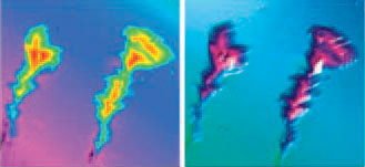 |
| Fig 1: Scratches in a hard nano-composite layer on silicon before (left) and after leveling. |
| Hardness, Elasticity and Tensile Strength Tests |
| The system can be used to slowly increase the load over a defined period of time ('quasi-static indentation'), or to perform a dynamic test where the tip is accelerated towards the surface, depositing a large amount of energy on contact ('nano-impact'). The wear of materials can be assessed by moving the sample slowly to produce a scratch while applying either a constant or ramped load as the sample moves along (Fig. 1). The frictional properties of the surface are measured simultaneously. The system applies the force using electromagnetic actuation. |
| The NanoTest (Fig. 2) from Micro Materials Ltd. is suitable for use with a wide range of materials as it can apply forces of between 30 nN and 500 mN depending on the operating mode, and it can measure penetration depths of between 0.1 nm and 50 µm. This task is carried out by a high-resolution capacitive sensor, the PISeca sensor from PI. The capacitive sensor measures the penetration depth of the tip as a function of time. In static operation, the coil current and thus the load is measured at the same time, enabling a load-displacement diagram (Fig. 3) to be compiled. |
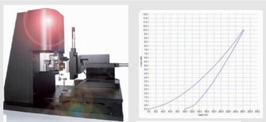 |
| Left: Fig 2 – The NanoTest nano-indentation system by Micro Materials Ltd. Right: Figure 3 – Load-displacement diagram. |
| In dynamic operation, the load is derived from the effective acceleration of the loading head. |
| Scanning Probe Microscopy Optimizes the Evaluation |
| The indentation method employed by the NanoTest can be combined with an imaging technique to investigate the sample surface pre and post indentation. The indentation tip is moved row-by-row in a defined grid across the surface of the sample, that is, the sample surface is scanned. The displacement of the tip is recorded point-by-point and used to generate a three-dimensional image of the sample surface which can be evaluated with the appropriate software – also developed by Micro Materials (Fig. 4). |
| This combination of indenter and scanning probe microscope thus provides a quick method for assessing the sample surface. It is also possible to perform measurements at different locations without a great deal of effort. |
| A P-527 piezo-based nanopositioning system (Fig. 5) from PI provides the motions in the X and Y axes which are required for the scan. Its 200 x 200 µm scanning range allows accurate statements to be made about the properties of the contact area and its surroundings. Thanks to the positioning accuracy of less than 3 nanometers a high positional resolution for the scan is guaranteed. |
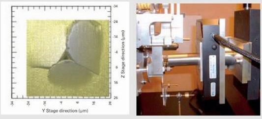 |
| Left: Fig 4 – Surface profile around the indent point of the tip, derived from a scan with the nanopositioning system. Right: Figure 5 – Integration of a piezo-based nanopositioning system with a 200 x 200 µm large scanning range with the NanoTest. |
| This means, critical loads are accurately assigned to a defined position which in turn allows conclusions to be drawn about the local material properties, and the high number of closely packed measuring points make it possible to investigate very small samples (Fig. 6). |
| Nanometrology: Capacitive Position Sensors |
| The absolute measuring capacitive sensors operate with resolutions down to the sub-nanometer range, and provide depth information without coming into contact with the sample. They operate without wear and hysteresis, and do not affect the application itself. |
| A simple physical principle is at the heart of capacitive metrology: When a voltage is applied, a homogenous electric field is produced between the plates of a capacitor. When the gap between the plates changes, the output signal from the metrology electronics changes proportionally. Capacitive position sensors are available in two different basic designs, i.e. as one-electrode or two-electrode systems. The NanoTest uses sensors with only one electrode. A conductive disc mounted on the rear of the indentation tip serves as the second electrode. |
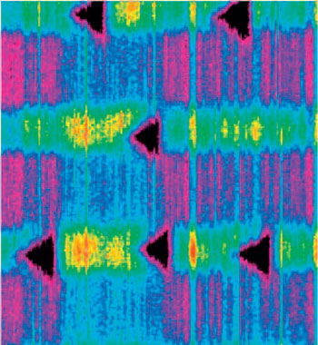 |
| Fig 6: Precise positioning of indentations measuring 60 nm across and 10 nm deep. |
| About Micro Materials |
| A particularly flexible nano indentation system originates from Micro Materials Ltd. based in Wrexham/UK. The Nano-Test (Fig. 2) is used as an informative testing system in various fields world-wide. It is not only used in research and development but also in production and the testing of finished products. |
| The current MML NanoTest system offers a range of methods for materials characterization, including nanoindentation, nano-impact and nano-scratch and wear measurements. It is in use in leading universities and industrial laboratories all over the world. |
| For more information on the NanoTest system visit http://www.micromaterials.co.uk. For more information on piezo nano-positioning systems and capacitive sensors visit www.pi.ws or http://www.nanopositioning.net |
| By PI (Physik Instrumente) L.P |

Become a Spotlight guest author! Join our large and growing group of guest contributors. Have you just published a scientific paper or have other exciting developments to share with the nanotechnology community? Here is how to publish on nanowerk.com. |
