| Posted: |
(page 2 of 4) |
| A suitable AFM tip is brought into the optical near-field above the sample and illuminated by continuous or pulsed light at wavelengths ranging from the visible to the infrared. The incident radiation is locally enhanced at the tip apex, subsequently interacts with the sample and is scattered back into detectable far-field radiation. |
| A suitable detection scheme analyzes the light in the far-field allowing the measurement of optical signals like Raman, infrared, or non-linear second-harmonic data with lateral resolution determined by the size of the scattering source, i.e., the AFM tip. These measurements can be accomplished in transmission or reflection geometry, enabling characterization of transparent and opaque samples, respectively. |
| The Raman signal from the <20nm region defined by an AFM tip normally would be vanishingly small, considering the inefficiency of the Raman process in addition to the reduction of the collection area from several squaremicrons for a far-field illumination spot to a submicronsquare area for a typical AFM tip. In contrast, the tip apex locally enhances both the incident laser excitation as well as the induced Raman polarization. |
| The enhancement can be achieved by combining certain metal tips with particular excitation light sources, such as a silver tip with green light and a gold tip with red light. |
| In general coinage metals work well as materials for tip-enhanced Raman scattering (TERS) tips because they exhibit a surface plasmon resonance in the visible range of the spectrum and thus can be excited by the incident laser beam. This strong enhancement is what makes Raman spectroscopy at the nanometer scale feasible.7 |
| Incidentally, a side illumination scheme as shown in figure 2 has been shown to generate the highest enhancement factor for TERS.8,9 Because of the strong localization of the electromagnetic field around the tip, TERS exhibits a much higher surface sensitivity than far-field Raman spectroscopy.10 |
| In Raman, the polarization of the electromagnetic field along the tip axis has an effect on the selection rules for Raman emission. This can become important when comparing far-field and near-field data.11 |
| The following experiment demonstrates the importance of polarization control of the incident beam for TERS (see figure 3). An etched gold wire was used as a TERS tip and glued to a tuning fork. The tuning fork was operated at resonance so that the tip was oscillated at an amplitude of about 1nm parallel to the surface. This non-optical feedback method is often referred to as shear-force feedback and keeps the tip in feedback above a Graphene sample without making intermittent contact.12 Using a waveplate, the incident light polarization was varied from being along the tip axis (p-polarized) to being perpendicular to the tip axis (s-polarized). The spectrum exhibits the D- and G-band region from 1300 to 1600cm-1, and one can see the enhancement effect almost disappeared when s-polarized illumination was used. |
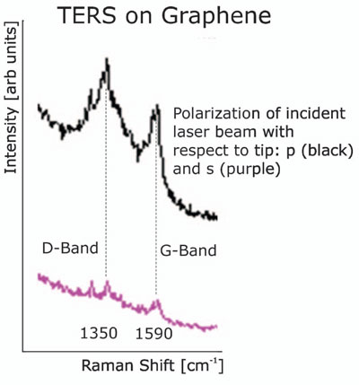 |
| Figure 3. TERS spectra of graphene obtained using a gold tip and tuning fork AFM feedback. It is evident that the TERS effect only happens when the incident light was polarized along the tip axis (p-polarized) and not perpendicular to it (s-polarized). (The authors would like to thank Samuel Berweger/University of Colorado for helping acquire the spectrum.) |
| Tip-enhanced spectroscopies such as TERS open the door to a whole new field of research. The improvement in spatial resolution is the obvious gain one expects from combining traditional far-field spectroscopies with atomic force microscopy, but there is also a higher sensitivity to surface features. The difference in selection rules between near- and far-field experiments indicates that TERS is similar to conventional Raman spectroscopy but does not just yield the exact same information on a smaller length scale. |
| Instrumentation for a Combined AFM-Raman System |
| The biggest challenge in a combined instrument enabling Raman spectroscopy and nanoscale surface characterization is to avoid compromising the performance of either. Several design factors need to be considered. |
| Optical interference ? Typically, Raman measurements are carried out using excitation in the visible regime. To allow parallel, simultaneous operation of the spectrometer and the AFM, the wavelength of the AFM beam-bounce system should be changed to the near-IR so as to not interfere with optical measurements. A better solution is to employ a non-optical feedback system, such as STM or tuning fork feedback.12 |
| Noise ? Spectrometer systems often employ several lasers that may be cooled by noisy external fans or water cooling systems. They also may radiate heat in the proximity of the AFM. Both of these effects can negatively affect AFM performance. Noise from fans can couple into the AFM and cause instabilities in the feedback loop. Temperature changes will cause the AFM to drift and make it extremely difficult to keep the tip in the selected field-of-view. |
| Measurement location ? To operate without a compromise in performance, the sample could be shuttled between the AFM and the Raman spectrometer as shown in Figure 4. |
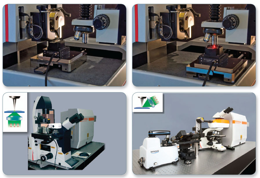 |
| Figure 4. View of the Dimension Icon stage and optics arm of the Raman microscope for co-located AFM-Raman measurements (shown on top). The Icon stage shuttles the sample between the AFM head (left) and the Raman objective (right). The red spot emanating the objective is the Raman laser illuminating the sample during a Raman measurement. Photos of the sample-scanning Innova-IRIS and Catalyst-IRIS systems for correlated and TERS imaging are shown on bottom. (click image to enlarge) |
| However, to achieve the benefits of both the AFM?s high spatial resolution and TERS, the sample should be scanned underneath the tip, as is done on Bruker?s Catalyst and Innova AFMs. This is because the laser beam exciting the plasmon resonance in the AFM tip must be focused onto the tip during the imaging process, thus forcing the AFM imaging to be accomplished by sample scanning. For certain non-TERS co-localized AFM and Raman measurements, i.e., the execution of an AFM and micro-Raman experiment on the sample location, a tipscanning AFM, such as Bruker?s Dimension Icon, can be employed. These co-located measurements do not rely on the near-field enhancement of the AFM tip and are straightforward to perform and interpret as functionalities like ScanAsyst? software automation can be used.13 |
| Continue to next page (3 of 4) |
|
|

Become a Spotlight guest author! Join our large and growing group of guest contributors. Have you just published a scientific paper or have other exciting developments to share with the nanotechnology community? Here is how to publish on nanowerk.com. |
