| Posted: Jun 02, 2015 |
Taming the blackbody with thermal wells |
| (Nanowerk Spotlight) The blackbody radiation law – formulated by German physicist Max Plank in 1900 – famously helped to resolve the ultraviolet catastrophe (a prediction of classical physics that an ideal black body at thermal equilibrium will emit radiation with infinite power). It has since been used to predict the spectrum and intensity of thermal radiation as a function of the object temperature. Likewise, the object temperature can be discerned from its thermal emission spectrum, making this relation a valuable tool for astronomic observations. |
| According to Planck’s law, the emittance of a non-reflective black object – a blackbody – defines the maximum level of thermal emittance from an arbitrary object. |
| Planck’s law has been challenged in recent decades by predictions and successful demonstrations of the radiative heat transfer between objects separated by nanoscale gaps that deviate significantly from the law predictions. |
| Despite the seeming contradiction of these observations with the law in its form derived by Max Planck, there is nothing surprising in the law ‘breakdown’ at short distances. In fact, Planck himself was well aware that the law bearing his name is valid only when ‘the linear dimension of all parts considered, as well as radii of curvature of all surfaces... are large compared with the wavelength of the ray considered.’ |
| However, to take advantage of the increased near-field radiative heat transfer above the blackbody limit, the two objects need to be separated by ultra-narrow gaps on the order of microns or even nanometers. |
| This limitation significantly complicates practical device designs based on exploiting this principle. |
| In new work published in the June 1, 2015 online edition of Scientific Reports ("Thin-film ‘Thermal Well’ Emitters and Absorbers for High-Efficiency Thermophotovoltaics"), Jonathan Tong, a PhD student at MIT working under the supervision of Dr. Svetlana V. Boriskina and Prof. Gang Chen, demonstrates another way to modify the object thermal emission spectrum and to force it to deviate from the one predicted by Planck’s law. |
| This goal is achieved by reducing the dimensionality of the emitter itself. |
| The MIT researchers built upon the concept of confining electrons in quantum wells, wires and dots, and proposed an analogous way to tailor thermal emission by engineering confined photon states in two- and three-dimensional potential traps, including wells, wires, and dots (Fig. 1). |
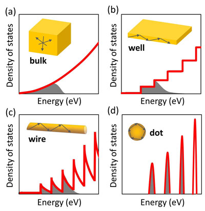 |
| Figure 1. Spatial confinement concentrates photon states and enhances thermal emission at select frequencies. Red lines: density of optical states in low-dimensional emitters; Shaded areas: thermal distribution of photons in (a) bulk material, (b) wells, (c) wires, and (d) dots. (Image: Dr. Boriskina) |
| To achieve the required level of photon confinement, the dimensions of the radiating objects should be on the order of or below the thermal wavelength predicted by Planck’s law. |
| The authors point out that the new concept does not challenge the validity of Planck's law, but rather applies it properly to a situation where the photon density of states of the emitter strongly deviates from the photon density of states of bulk matter. This is in direct analogy with the modification of electron density of states in their quantum counterparts. |
| Most importantly, the emission spectrum of thermal wells, wires and dots deviates from Planck’s law predictions not only in the near field, but also in the far field, which significantly expands the range of their applications. |
| In their paper, the MIT team applied this new concept to predict a new way to improve performance of a thermophotovoltaic energy converter. |
| TPV conversion platforms harvest thermal radiation from hot emitters and convert it into electrical current in a photovoltaic (PV) cell. However, the broad thermal emission spectrum is not optimally matched to the PV cell absorption window. Ideally, emission of long-energy photons that cannot be utilized by the PV cell needs to be suppressed, and emission of photons with the energies just above the PV cell bandgap enhanced. |
| The MIT team reports on a new TPV system design, consisting of a thin-film thermal emitter and a thin-film PV cell, which support quantized optical modes trapped inside the material by total internal reflection. The researchers explain that dispersion characteristics of these confined modes lead to resonant enhancement of their photon density of states, which in turn modifies their thermal emission and absorption, both in the near- and far-field (Fig. 2a). |
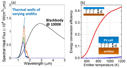 |
| Figure 2. (a) Modification of the thermal emission spectra enabled by the spatial confinement of photons in thermal wells, (b) resulting in the improvement of the TPV system energy conversion efficiency over its bulk counterpart (Image: Dr. Boriskina) |
| More importantly, these confined modes exhibit cut-off frequencies at longer wavelengths, enabling suppression of emission of photons with energies smaller than the band gap of the PV cell. Simultaneously, in a thin PV cell, photo-excited electrons and holes need to travel shorter distances, which reduces their bulk recombination losses and yields a lower saturation current in the PV cell. |
| By improving the spectral selectivity and reducing the saturation current, the 'thermal well' effect proposed by the MIT team theoretically offers enhancement of the TPV system energy conversion efficiency by over an order of magnitude compared to both the bulk limit and the Shockley Queisser limit for a blackbody emitter at the same temperature (Fig. 2b). |
| For a thin-film Ge emitter and a thin-film GaSb PV cell, the maximum TPV energy conversion efficiency was predicted to be as high as 38.7% at an emitter temperature of 1000 K and gap separation of 100 nm. In the far-field limit, this efficiency decreases to 31.5%; however, this is still significantly higher than the Shockley Queisser limit even for a blackbody emitter at a temperature of 2000 K. |
| These predictions offer a significant improvement in the TPV system performance over prior designs based on the use of surface polariton modes coupling in the near field, which are challenging to realize in a practical system. |
| The new TPV system design also does not require nanoscale patterning of the emitter and PV cell surfaces, and thus offers a simple low-cost solution to improve the performance of future TPV systems. |
| This work was supported by the U.S. Department of Energy, Office of Basic Energy Sciences, Division of Materials Science and Engineering Award No. DE-FG02-02ER45977 (for the thermal emission manipulation) and by the ‘Solid State Solar-Thermal Energy Conversion Center (S3TEC)’, funded by the US Department of Energy, Office of Science, and Office of Basic Energy, Award No. DE-SC0001299/DE-FG02-09ER46577 (for thermophotovoltaic applications). |
|
By Dr. Svetlana V. Boriskina, MIT
|

Become a Spotlight guest author! Join our large and growing group of guest contributors. Have you just published a scientific paper or have other exciting developments to share with the nanotechnology community? Here is how to publish on nanowerk.com. |
