| Posted: Jan 07, 2016 |
Toward the automation of plasmonic design |
| (Nanowerk Spotlight) Metal nanoparticles, when excited at optical frequencies, may experience localized surface plasmon resonances, which determine enhanced local electric fields, increased scattering cross sections, and high sensitivity to the environment refractive index. Thanks to these unique properties, they are now widely utilized especially in biomedical sciences and engineering. |
| Researchers from the the University of Napoli 'Federico II', the University of Utah, and the Boston University, have now conceived and demonstrated a new method to fully automate the design of metal nanoparticles. |
| The current praxis of designing plasmonic devices by hand, mainly guided by qualitative arguments significantly limits the accessible design space and consequently the achievable performances. Furthermore, the geometries suggested by these approaches require additional refinements by full-wave electromagnetic solver carried out by sweeping the relevant geometrical parameters through a given range. |
| This time-consuming design process exacerbates the delay between proof-of-concept plasmonic devices and marketable technology, which has become apparent in the last few years. |
| On the other hand, the automation of the plasmonic design by rigorous inverse-design strategies could make very large search-spaces easily accessible, where the user could look for a specific nanostructure meeting specific needs with unparalleled accuracy. |
| In a recent paper in ACS Photonics ("Inverse Design of Metal Nanoparticles’ Morphology"), the authors propose a rigorous inverse design method to engineer the shape of metal nanoparticles according to a pre-assigned objective function, coupling an efficient global optimization algorithm to a 3D full-wave, electromagnetic solver. |
 |
| Exemplificative shapes generated by the 3D Gielis’ superformula (Artistic impression: University of Napoli 'Federico II') |
| Contrary to the solution of a direct problem, which simply aims at determining the electromagnetic field scattered by a given particle of prescribed shape, size, and composition under assigned excitation conditions, the inverse-design problem consists of determining the characteristics of the scattering object, based on the desired properties of the scattered electromagnetic field. |
| The authors described the search space by using a simple, unifying equation, the Gielis superformula. J. Gielis introduced its mathematical expression about a decade ago ("A generic geometric transformation that unifies a wide range of natural and abstract shapes") and proved it to be extremely effective to describe a variety of forms and patterns occurring in nature, including cells, tissues, stems, flowers, shells, starfish, galaxies, and DNA molecules. |
| The researchers used their proposed strategy to design the morphology of three-dimensional nanoparticles, maximizing the electric field averaged on their surface, which plays a fundamental role in the surface enhanced Raman scattering (SERS) and for the subwavelength focusing of light. |
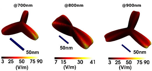 |
| Inverse-designed gold nanoparticles and corresponding distribution of electric field magnitude on their surface. The particles have been optimized aiming at maximizing their electric field averaged on their surfaces. The particles are excited by a x-polarized plane wave of unit electric field magnitude (1 V/m) propagating along the z-axis at wavelength 700 nm,800 nm, 900 nm. (Image: University of Napoli 'Federico II') |
| The automation of nanoplasmonic design enables the fine engineering of numerous nanoscale optical devices such as plasmon-enhanced Raman sensors, photodetectors, light sources and more efficient nonlinear optical elements for on chip integration. |
|
Source: University of Napoli 'Federico II'
|

Become a Spotlight guest author! Join our large and growing group of guest contributors. Have you just published a scientific paper or have other exciting developments to share with the nanotechnology community? Here is how to publish on nanowerk.com. |
