| Posted: Jan 11, 2016 |
Box-shaped graphene � a novel nanostructure |
| (Nanowerk Spotlight) A scientist from the Institute of Physical Problems named after F. V. Lukin in Zelenograd, Russian Federation, has discovered a previously unknown three-dimensional nanostructure consisting of graphene sheets. |
| The researcher, Dr. Rostislav Lapshin, a staff scientist at the institute, has reported his findings in the January 1, 2016 edition of Applied Surface Science ("STM observation of a box-shaped graphene nanostructure appeared after mechanical cleavage of pyrolytic graphite"). |
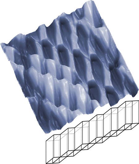 |
| Box-shaped graphene – a three-dimensional nanostructure consisting of graphene sheets. (Image: courtesy of Dr. Rostislav V. Lapshin, Institute of Physical Problems) |
| Graphene is a single monolayer of carbon atoms forming a hexagonal two-dimensional crystal lattice. The discovered nanostructure is a multilayer system of parallel hollow channels with quadrangular cross-section extending along the surface. |
| The thickness of the channel walls/facets of the nanostructure is about 1 nm, the width of the channel facets is approximately 25 nm, and the channel length reaches at least several hundreds of nanometers. |
| Dr. Lapshin explains: "Actually, graphite crystal can be thought of as a stack of graphene sheets. Graphite surface under a scanning tunneling microscope (STM) looks 'dull' and uniform. Usually, one may see plain areas of surface of several microns in size bounded by cleaving steps without any features. Only rarely does the familiar 'landscape' contain something unusual, for example, a carbon fiber, a superlattice or a dislocation network." |
| The discovered nanostructure looked so extraordinary that it took some time to understand what it actually was. The structure was dramatically different from whatever had previously been observed on graphite. |
| Only after performing additional measurements and analysis of the images, it became clear that this was a system of hollow nanosized channels extending along the surface with wall thickness less than 1 nm. The estimated value of thickness as well as the quadrangular cross-section of the channels unambiguously indicate that the channel walls/facets are graphene planes. |
| After clarifying the geometry and sizes of the discovered objects, Dr. Lapshin set out to understand how they had been formed. Several hypotheses were suggested, but all of them appeared to be either too complicated or too 'fantastic'. |
| Finally, a rather simple, if not to say elegant, solution was found, which is based on a series of mechanical deformations of graphite, which is layered by nature. |
| "In summary, it appears that this is the formation mechanism," Lapshin explains: "During graphite cleavage, a compressive stress directed along the surface appears in the thin surface layer. As the cleaving front moves on, the compressive stress causes, first, elastic bending of this layer at a small section, and then plastic deformation of the layer with its simultaneous splitting into graphene sublayers. The last two transformations result in a nanofold formation. At the final stage, the split graphene sublayers slide in the nanofolds relative to each other resulting in formation of the nanochannels arranged in stacked layers." |
| Since the nanochannels have a quadrangular cross-section, the detected graphene nanostructure has been named box-shaped. It is noteworthy that the box-shaped graphene (BSG) nanostructure contained so many interesting features that just three STM scans were enough to make substantial conclusions about the structure and its main parameters. |
| Even the preliminary analysis of the BSG nanostructure has shown good prospects of its use in various devices. Here are some of the possible applications: ultra-sensitive detectors; high-performance catalytic cells; nanochannels of microfluidic devices (molecular sieving, DNA sequencing and manipulation); high-performance heat sinking surfaces; rechargeable batteries of enhanced performance; nanomechanical resonators; electron multiplication channels in emission nanoelectronic devices; high-capacity sorbents for safe hydrogen storage. |
|
Source: Science and Technology of the Russian Federation (STRF). English translation by Oleg E. Lyapin.
|

Become a Spotlight guest author! Join our large and growing group of guest contributors. Have you just published a scientific paper or have other exciting developments to share with the nanotechnology community? Here is how to publish on nanowerk.com. |
