| Posted: Apr 17, 2006 |
Manipulating spheres for nanowire growth: two steps better than one |
| (Nanowerk Spotlight) Fabrication of nanowires arrays with different patterns and separations is a major concern of the nanowire community. For this purpose, a catalyst template, which is usually a metal nanoparticle array, is needed to guide the nanowire growth. |
| Among various approaches to catalyst templates, nanosphere lithography (NSL) is a classical one because of its low cost and high efficiency. This technique works nearly perfectly on Si, glass and sapphire, and has been widely used for structuring substrates with a hexagonal array of various nanomaterials, including ferroelectric, magnetic, and catalytic metal dots for growth of 1-D nanomaterials (for example, carbon nanotubes and ZnO nanowires). Previous demonstration of ZnO nanowire fabrication by NSL took place on sapphire, which is an insulating, and thus a less desirable substrate in terms of the device applications of nanowires. |
| In contrast, in a recent paper in Journal of Crystal Growth "Well-ordered ZnO nanowire arrays on GaN substrate fabricated via nanospheres lithography", first-authored by Hongjin Fan, a modified NSL technique was applied on GaN for ZnO nanowire growth. GaN is a ideal substrate because of its similar optical bandgap energy (∼3.4 eV) and low misfit of the lattice constant (1.9%) to ZnO, and because of the potential for p-GaN/n-ZnO nano heterojunctions. |
| However, the GaN surface is hydrophobic which retards a direct self-assembly of polystyrene spheres. To overcome this problem, we applied an old "mask transfer" technique, where an additional step was used followed by transferring the sphere layers from glass substrate to GaN surface. |
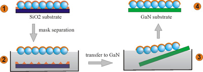 |
| Cartoon of the “mask transfer” process. (1) PS spheres are self-assembled to mono- or bilayer on SiO2 substrate. A relatively thick (~50 nm) gold film was then deposited on top of the PS layers in order to (i) stabilize the PS layer for the subsequent transfer process; and (ii) reduce the gap between the spheres. (2) The membrane of gold stabilized PS spheres is detached from the SiO2 substrate in water. (3-4) The membrane is then transferred onto GaN simply by fishing. (Source: Max-Planck-Institute of Microstructure Physics) |
| Advantages of this "mask transfer" technique include: (1) the transfer is substrate friendly since the hydrophilicity problem is bypassed; (2) the inter-sphere holes are narrowed by the metal coating which results in one-to-one growth (i.e., nearly a single wire at each catalytic Au dot site) and well separation of the nanowires. |
| By this technique, we obtained ZnO nanowires which exhibit truly vertical alignment and well separation, and two types of patterns corresponding to a mono- and bilayer of spheres, respectively. This is highly desirable for size-specific individual NW arrays on conductive substrates as needed for device applications such as sensor arrays or field emitter arrays. By contrast, sapphire substrates do not offer these specifics. |
| Recent advances in NSL allow more complicated assembly of the spheres by adjusting the inter-layer orientations, combining different-sized spheres, or additional etching process. This gives us more choices in type of patterns and lattice constants. Therefore, we can expect more flexibility in the patterned growth of ZnO nanowires. This reinforces the great application potential of this fascinating material. Of course, although demonstrated here is ZnO, this method is readily extendable to other materials on corresponding lattice-matched substrates. |
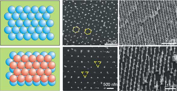 |
| Left column: cartoon of mono- and bilayer polystyrene spheres through self-assembly. Middle column: top view of the ZnO nanowire arrays exhibiting honeycomb and triangular pattern, respectively. Right column: corresponding perspective view of the ZnO nanowire arrays. (Source: Max-Planck-Institute of Microstructure Physics) |
| It is worth mentioning that the use of a small-volume reaction tube and the low substrate temperature is essential in our method. This sounds a minor point but actually turns out to be a key issue. Small-sized gold nanoparticles are very mobile at elevated temperature, which destroys the pattern. The small tube in the big reaction chamber maintains a high vapor concentration above the substrate, which effectively reduces the temperature required for nanowire growth. |
| While the nanowire community is gaining more control in the growth of nanowires, a further step to patterning becomes simply either a reuse of many conventional lithography techniques (e.g., photo- and electron-beam lithography, AFM tip manipulation), or applying modern unconventional nanopositioning techniques (e.g., phase-shift or imprint lithography). A recent review article titled "Semiconductor nanowires: from self-organization to patterned growth" will be published in the April 25,2006 online issue of the journal Small. |
| More details about the setup can be found in other related papers from our group homepage. The group, led by Dr. Margit Zacharias of the Max-Planck-Institute of Microstructure Physics (Germany), has been focusing on using GaN epilayers as ideal substrates for ZnO nanowires. They have published 12 articles on this topic since 2004. |
| By Hongjin Fan, Max-Planck-Institute of Microstructure Physics, Halle, Germany. |

Become a Spotlight guest author! Join our large and growing group of guest contributors. Have you just published a scientific paper or have other exciting developments to share with the nanotechnology community? Here is how to publish on nanowerk.com. |
