| Posted: Dec 28, 2016 |
Consistent-chirality carbon nanotube tangles with high on-current in transistors |
| (Nanowerk Spotlight) Carbon nanotubes (CNTs) are expected to replace silicon as the next generation semiconductor materials owing to their perfect structure and excellent properties. IBM has proposed a technical standard for CNT-based electronics, which singled out the necessity of a high density of up to 125 CNTs µm-1 in tandem with a high semiconducting selectivity of up to 99.9999% for single-walled CNT arrays. |
| Therefore, in the past decades, great effort has been applied on the controllable synthesis of ideal CNTs. |
| However, it’s almost impossible to directly synthesize pure semiconducting CNTs by an in situ catalytic reaction alone, without any post-separation, when only small amounts of metallic CNTs may cause catastrophic device shorting failures. |
| That is why the synthesis of CNTs with consistent chirality and high density is facing a bottleneck. |
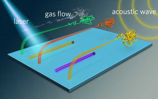
| A group of researchers in China have creatively proposed a novel method by entangling an individual decimeter-long CNT with a diameter of 2 nm into a large tangle with high density and consistent chirality. |
| The team, led by professor Fei Wei from Tsinghua University, has published their findings in ("Acoustic-assisted assembly of an individual monochromatic ultralong carbon nanotube for high on-current transistors"). |
 |
| Schematic illustration of the synthesis of CNT tangles assisted with acoustic waves. (Reprinted with permission by AAAS) |
| "Controlled growth of CNTs with high quality has always been our research focus," says Pro. Wei, whose team, in previous work, has achieved record high thousand-ton output of CNTs and synthesized the half-meter long CNTs. "We have demonstrated the chiral-consistency of an individual decimeter-long CNT, but these as-synthesized horizontally aligned ultra long CNTs possess different chirality and tip-growth-mode-determined low density." "The motivation for this work has been to change the problem of manipulating or separating individual nanotubes into an easier problem for millimeter scale tangles," he continues. "Besides, it also provides a novel paradigm for the synthesis of chirality-specific CNT aggregates." |
| "Assisted by acoustic waves, we curled each individual ultra long CNT into large tangles and the key for realizing the entanglement is our newly-designed layered rectangular reactor," says Zhenxing Zhu, a doctor at Tsinghua University and the paper’s first author. "Gas flow stability is important for controlling the horizontally aligned morphology for ultra long CNTs synthesized via the chemical vapor deposition method. The new reactor designed with a large width-to-height aspect ratio led to a reduction of velocity fluctuation and a significantly stabilized gas flow during the reaction. So the floating CNTs will get more sensitive to external interference and easily curl into tangles under the effect of acoustic waves." |
| "Another benefit of this new reactor is the capability of wafer-scale synthesis of ultra long CNTs. We characterized ultra long CNTs and tangles directly on silicon wafers with Rayleigh or Raman spectra, indicating the chiral-consistency and monochromatic," Pro. Wei adds. "The scale of tangles is closely related to frequency of sound and gas velocity, which can be described with a Strouhal number model initially used for tail or wing kinematics of swimming and flying animals. We think this minimally consumed energy phenomenon also exists at the nanoscale." |
| As the researchers showed, these tangles made of triple-walled CNTs possess an area ranging from 1×10⁴ to 3×104 µm2 and a density of 1000 segments per 100 µm. |
| Despite of that, transistors fabricated with one CNT tangle showed an on/off ratio of 103 to 106 with 4-mA on-state current, showing a feasible method for compatibility between high semiconducting purity and high areal density for CNTs. |
| Moreover, this is also the highest on-state current recorded so far for single CNT-based transistors. |
| According to Prof. Wei, "this is only the first step of our roadmap for wafer-scale applications of CNT tangles. We will synthesize more and larger tangles directly on wafers so that the separation can be performed on a larger scale. Also, these tangles can be post-densified to improve their density further. Then, the ones with the same color can be enriched on the designated substrate and high-performance devices can be fabricated on them." |
|
By Zhenxing Zhu, PhD, Department of Chemical Engineering, Tsinghua University, Beijing 100084 (zhenxing1013hg @ 163.com)
|

Become a Spotlight guest author! Join our large and growing group of guest contributors. Have you just published a scientific paper or have other exciting developments to share with the nanotechnology community? Here is how to publish on nanowerk.com. |
