| Posted: Jan 09, 2018 |
A a new cooling mechanism for electronic components made of graphene deposited on boron nitride |
| (Nanowerk Spotlight) Researchers in the optics and mesoscopic physics teams from the Laboratoire Pierre Aigrain (LPA) based in the ENS Physics department in Paris (France) discovered a new cooling mechanism concerning electronic components made of graphene deposited on boron nitride. The efficiency of this mechanism allowed them to reach electric intensities at the intrinsic limit of the laws of conduction. |
| From supercalculators to smartphones, industries are confronted with a major challenge: how to evacuate more and more heat to prevent deterioration or even destruction of electronic components. The laws of physics are cruel: Increasing the density of components on a chipset implies increasing dissipation and thus heat. |
| Nowadays, with the advances in 2D material devices, this question becomes particularly critical since components can be only one atom thick. In this context, by producing a graphene-based transistor deposited on a boron nitride substrate, physicists from the Pierre Aigrain Laboratory (CNRS / ENS / UPMC / Paris Diderot University) have discovered a new cooling mechanism 10 times more efficient than basic heat diffusion. |
| This new mechanism, which exploits the two-dimensional nature of the materials opens a "thermal bridge" between the graphene sheets and the substrate. Researchers have demonstrated the effectiveness of this mechanism by imposing in graphene levels of electrical current still unexplored, up to the intrinsic limit of the material and without any degradation of the device. |
| This result, published in Nature Nanotechnology ("A graphene Zener–Klein transistor cooled by a hyperbolic substrate"), is an important step towards the development of graphene-based high-frequency electronic transistors. |
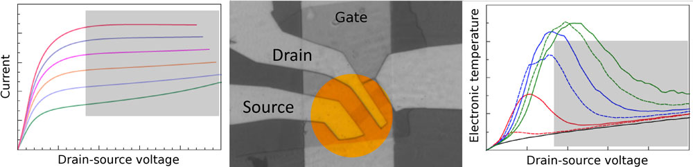 |
| Current-voltage (left) and temperature-voltage (right) characteristics of a graphene on boron nitride transistor. The transistor effect is visible by modulation of the current as a function of the gate voltage in the Zener-Klein tunnel transport regime (greyed out). It corresponds to a remarkable drop in the electronic temperature associated with the emission of hyperbolic polaritons in boron nitride. (Image: Pierre Aigrain Laboratory) (click on image to enlarge) |
| To perform this experiment, physicists first made a graphene-based transistor. For this purpose, they deposited the graphene on a large boron nitride crystal a few tens of nanometers thick itself deposited on a gold plate used as a thermostat. |
| They then operated this transistor at increasing electrical intensities and measured both the temperature of the electrons in the transistor channel and that of the crystal. The electronic temperature has been deduced from the measurement of the high frequency fluctuations of the electric current. The temperature of the boron nitride crystal was measured by Raman spectroscopy. |
| Their first surprise was to observe that only the electrons heat up, thus sparing the crystalline structure of the material. The researchers then observed the ignition of an ultra-efficient electron cooling mechanism beyond a voltage threshold. |
| They explained this phenomenon by the dielectric anisotropy of the boron nitride layer. This anisotropy gives this insulator the remarkable property of having mixed light-vibration modes called hyperbolic polaritons that propagate in the thickness of the material in a regime forbidden to most other insulators. |
| These "hyperbolic" modes open a real thermal bridge between the graphene and the rear electrode guaranteeing a cooling 10 times more effective than the mere diffusion of heat. |
| The LPA team has shown that the efficiency of this mechanism is increased tenfold when the transistor enters the Zener-Klein regime, obtained under a very strong electric field in high electron mobility graphene. In this new regime, of particular interest for high frequency amplification applications, the electrons are directly pumped from the valence band to the tunneling conduction band. Under these conditions, they couple optimally to hyperbolic modes, allowing heat to pass directly to the substrate without damaging the graphene network. |
|
Source: Pierre Aigrain Laboratory
|

Become a Spotlight guest author! Join our large and growing group of guest contributors. Have you just published a scientific paper or have other exciting developments to share with the nanotechnology community? Here is how to publish on nanowerk.com. |
