| Posted: Jul 30, 2018 |
Femtosecond laser creates nanoelectronics on graphene |
| (Nanowerk Spotlight) No other material possesses greater promise to revolutionize electronics as graphene. Each year brings new discoveries in electronic, optical and mechanical properties of graphene. The question that must be put on the table is what ground breaking technology would bring graphene to the industrial level. |
| Traditional CMOS technology cannot be directly merged with graphene applications. Photo- and electron-based lithographies, which are the main processess in today's semiconductor industry, requires use of polymers and harsh liquids that can drastically alter the initial properties of graphene. Thus graphene requires the development of novel processing technologies. |
| A team of researchers from AIMEN Laser Applications Centre (Spain), Forschungszentrum Jülich (Germany), and National Research University of Electronic Technology (Russia), has developed a method for direct, on-the-fly reconstruction of graphene properties. |
| The method is based on the treatment of graphene surfaces with ultrafast laser pulses. When the pulse length is on the order of femtoseconds, the thermal effects can be eliminated, giving way to photoinduced chemical reactions. |
| Indeed, this phenomena currently is employed in 3D printers operated by multiphoton (photochemical) polymerization of molecules under irradiation of ultrashort laser pulses. However, the above-described method is novel, hence the process behind it is still not precisely understood. |
| The scientists suggest that femtosecond laser treatment of carbon lattice generates high energy electrons that are further transferred to oxygen and water molecules in the vicinity of the graphene surface, turning them into active radicals. These radicals, in turn, interact with graphene – leading to partial oxidation and doping. |
| The research team has reported their findings in ACS Photonics ("Thermoelectrically driven photocurrent generation in femtosecond laser patterned graphene junctions"). |
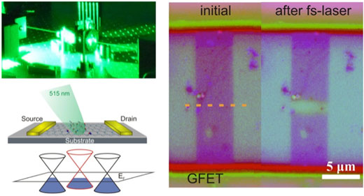 |
| Image shows the femtosecond laser system used in this work (upper left); schematic drawing of laser interaction with graphene transistor (central left); and energy band modification (bottom left) and optical view in artificial colors (optical profilometer, right) of graphene channel before and after laser processing. (Image: National Research University of Electronic Technology) |
| The researchers applied this method to produce photodetectors based on graphene field effect transistors. These detectors are shown to work at room temperature and do not need external cooling, providing sensitivity in a rather wide range of incident power. |
| Moreover, the team demonstrated that these photosensors are able to detect even single femtosecond laser pulses at energies below the detection limit of traditional silicon based photodetectors. |
| In spite of the extremely large photoresponse, unfortunately the process is slow in terms of relaxation into an equilibrium state, that is perhaps due to presence of charge traps at the interface with the underlying substrate. |
| Furthermore, it is of paramount importance to go beyond demonstration of a simple application (e.g. as compact photodetector), since the area of application of ultra-short laser pulses for tuning graphene properties is much greater. The AIMEN technological Center has filed a provisional patent on the technique. |
| This method can be also used for local graphene etching that can control not only doping levels of graphene but also its quantum confinement, leading to the creation of nanoribbons and nanomeshes and thus new logic electronic devices. |
| This study takes a first step towards the development of fully mask- and lithography-free methods for processing novel nanomaterials. Changing the environment like gas, or polymer coating may lead to other photochemical processes on graphene surfaces. Other 2D materials like phosphorene that provide very good photochemical activity could also be processed the same way. |
| The main benefit of the ultrafast laser method is that it can be used for all kinds of substrates and even on the surface of living organisms, paving the way for on-site development of integrated and implantable devices. |
|
A Nanowerk exclusive provided by National Research University of Electronic Technology
|

Become a Spotlight guest author! Join our large and growing group of guest contributors. Have you just published a scientific paper or have other exciting developments to share with the nanotechnology community? Here is how to publish on nanowerk.com. |
