| Apr 22, 2019 |
Quantum-material-based proton-irradiation-immune electronics for space travel |
| (Nanowerk Spotlight) The future of space exploration depends crucially on the development of new electronic technologies that are immune to space radiation, which consists primarily of protons, electrons, and cosmic rays. The penetrating energetic radiation of deep space produces negative impacts on not only biological entities but also the electronic systems of space vehicles. |
| Proton radiation damage is an important failure mechanism for electronic devices in near-Earth orbits and deep space. The plans to colonize Mars, explore possibilities of life on the satellites of Saturn and Jupiter, to increase efforts in high energy physics, and proton radiation use in medical fields, cannot be implemented without developing electronic technology, which is not susceptible to proton irradiation. |
| An interdisciplinary multi-university team of researchers led by Dr. Alexander Balandin, distinguished professor of electrical and computer engineering has recently demonstrated two-dimensional (2D) charge-density-wave (CDW) devices with a remarkable immunity to bombardment with 1.8 MeV protons to a fluence of at least 1014 H+cm-2. |
| The current-voltage characteristics of these devices did not change as a result of proton irradiation, in striking contrast to most conventional semiconductor devices or other two-dimensional devices. Only negligible changes were found in the devices’ noise spectra. |
| “We attributed the radiation immunity of these essentially all-metallic charge-density-wave devices to the quasi-two-dimensional nature of the electron transport in their nanoscale-thickness channels, high concentration of charge carriers in the charge-density-wave phases, and two-dimensional device design,” explained Balandin. “Such proton-irradiation-immune devices, capable of operating over a wide temperature range, can constitute a crucial segment of future electronics for space, particle accelerator and other radiation environments,” he added. |
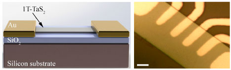 |
| Figure 1: Schematic diagram of the two-terminal 1T-TaS2 CDW device (right panel). An optical microscopy image of a representative 1T-TaS2 CDW device with Ti/Au (10 nm/100 nm) contacts. The scale bar is 3 µm. The devices were fabricated in the UCR Nanofabrication Facility. (The figure is courtesy of Adane Geremew and Professor Alexander A. Balandin, UCR) |
| In 2016, the University of California – Riverside (UCR) group developed the first CDW devices operating at room temperature ("Integrated trio of 2D nanomaterials unlocks graphene electronics applications"). Since that time, the UCR group demonstrated the use of CDW devices for information processing and communications. |
| The recent breakthrough showing the ability of CDW technology to withstand proton bombardment was made possible by combining expertise of Professor Alexander Balandin’s group in 2D device fabrication (UCR), proton testing expertise of Professor Daniel Fleetwood’s group (Vanderbilt University), electronic noise expertise of Dr. Sergey Rumyantsev (Polish Academy of Sciences, formerly from Ioffe Institute, Russia), materials synthesis expertise of Professor Tina Salguero (University of Georgia) and expertise in computer simulation of radiation defects of Dr. Alexander Fedoseyev (Huntsville, Alabama). |
| The results appeared in the journal Nanoscale ("Proton-irradiation-immune electronics implemented with two-dimensional charge-density-wave devices"). The first authors of the paper are Adane Geremew and Fariborz Kargar, members of Professor Balandin’s research group. |
| Protons cause ionizing damage and atomic displacements, resulting in device degradation and malfunction. Metal shielding of electronics increases the weight and cost of the systems but does not eliminate destructive single events produced by energetic protons. |
| Electronics capable of operating in high-radiation environments are also needed for monitoring nuclear materials, medical diagnostics, radiation treatments, nuclear reactors and particle accelerators. Unfortunately, modern electronics based on semiconductors – even those specially designed for radiation hardness – remain highly susceptible to proton damage. |
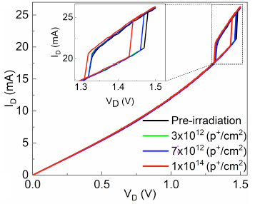 |
| Figure 2: Current-voltage characteristics of 1T-TaS2 device after different proton fluences. The inset shows the hysteresis window, which is the working part of the current-voltage characteristic of the device. The changes in the current and voltage are negligible even after the maximum proton irradiation dose. (The figure is courtesy of Adane Geremew and Professor Alexander A. Balandin, UCR) |
| “Two-dimensional charge-density-wave materials represent a class of quantum materials with very interesting properties. They are metals at elevated temperature and undergo various phase transitions at lower temperature. These transitions, triggered by electric field, are accompanied by changes in resistivity and hysteresis loops. We used these properties to make electronic switching devices without semiconductors,” explained Balandin. “It was amazing to see that high doses of proton radiation did not produce any noticeable effects on the device current-voltage or noise characteristics. Noise characteristics are important because they are sensitive to any sort of damage to the device material,” he added. |
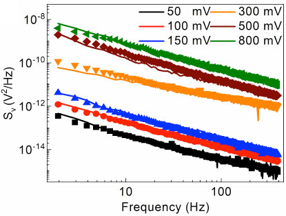 |
| Figure 3: The noise voltage power spectral density as a function of frequency for a representative CDW device before (solid lines) and after (symbols) proton irradiation. (The figure is courtesy of Adane Geremew and Professor Alexander A. Balandin, UCR) |
| “We hope that Elon Musk will notice these results and use the 2D CDW technology for his SpaceX and other space exploration projects,” said Balandin. “Naturally, the technology still needs major R&D efforts but the initial data are extremely promising,” he added. |
|
Provided by University of California - Riverside as a Nanowerk exclusive
|

Become a Spotlight guest author! Join our large and growing group of guest contributors. Have you just published a scientific paper or have other exciting developments to share with the nanotechnology community? Here is how to publish on nanowerk.com. |
