| Jul 05, 2019 |
Highly sensitive and controllable photodetector based on 2D BiOI nanosheets |
| (Nanowerk Spotlight) In recent years, two-dimensional (2D) materials have attracted tremendous attention due to their exotic physical and chemical properties. So far, the main research enthusiasm has been focused on the ones with single or binary elements, such as graphene and various transition metal dichalcogenides (TMDs). |
| Recently, the investigation of ternary layered compounds with 2D features has emerged. Compared to 2D elements and binary compounds, ternary layered compounds possess more tunability for physical and chemical properties due to more element species. Therefore, exploring the preparation methods and special properties of 2D ternary compounds is of great significance for enriching the 2D material library and expanding the application of 2D materials. |
| BiOI (a bismuth oxyhalide) is a ternary layered semiconductor with a bandgap of about 2.0 eV and good absorption character in the visible light range. Particularly, theoretical calculations indicate that 2D BiOI has a small electron effective mass of 0.36 me* and a high electron mobility of 771.19 cm2 V-1 s-1 at room temperature, manifesting its potential applications in micro- and nanoelectronic as well as optoelectronic devices. |
| At present, many nanostructures of BiOI, such as nanospheres and nanoparticles, were prepared by hydrothermal method and were used as a non-toxic photocatalytic material. However, research on the synthesis of large area atomically thin 2D BiOI single crystals and the investigation of their applications in photodetection have not been reported yet. |
| In addition, as we know, vacancies in semiconductor play a crucial role in their electrical properties. However, how to control these defects and how these defects affect the photodetector’s performance are not systematically studied. Understanding the special characteristics of the device will be helpful to find a way to adjust, even enhance the device performance based on these materials. |
| In a recent work, the research team of Professor Liping Feng at Northwestern Polytechnical University in China has reported a novel study on realizing the van der Walls epitaxy of large area 2D BiOI single crystal on mica substrates with lateral size over 100 µm by using space-confined chemical vapor deposition at lower temperatures (< 350°C). |
| Also, the researchers found that the confined method – substrate stacking – can optimize the reactant concentration in the confined space to achieve 2D growth of BiOI crystals between two stacked micas. |
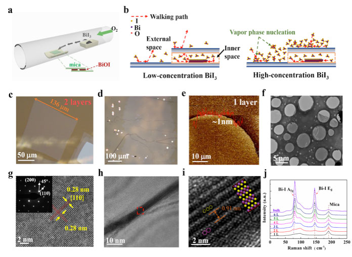 |
| Figure 1. Lattice structure and growth of layered BiOI nanosheets. (a) Schematic illustration of the CVD configuration for synthesizing BiOI nanosheets on mica with the precursors of BiI3 and O2. (b) Schematic illustration of space-confined mechanism for the growth of BiOI nanosheets at low (left) and high (right) concentration of BiI3. (c) OM images of large-area atomically thin BiOI nanosheets with thicknesses of 2 layers. (d) A continuous 2D BiOI polycrystalline film. (e) AFM image of monolayer BiOI and corresponding height profile. (f) Low-magnification TEM image of a square 2D BiOI nanosheet on holey carbon TEM grid. (g) HRTEM image of the BiOI nanosheet taken form c-axis. The lattice spacing of 0.28 nm was measured for (110) of BiOI and inset shows the SAED pattern. (h) HRTEM image recorded from the folded edge. (i) Magnified HRTEM image taken from red box in (h). (Image: Northwestern Polytechnic Institute) (click on image to enlarge) |
| Additionally, photodetectors based on 2D BiOI nanosheets were fabricated for the first time. The photoresponsivity of the photodetector is around 2.6×10⁻² A/W under 473 nm light, the detectivity can reach up to 8.2×10¹¹ Jones, and the switching ratio is close to 105. |
| Moreover, under the irradiation of 254 nm UV light, the dark current and photo current of the photodetector based on 2D BiOI were found to increase because amount of oxygen vacancies were introduced into ultrathin BiOI crystals. That is to say, UV light irradiation can tailor the component of 2D BiOI crystal and thus adjust the electrical properties of the device. |
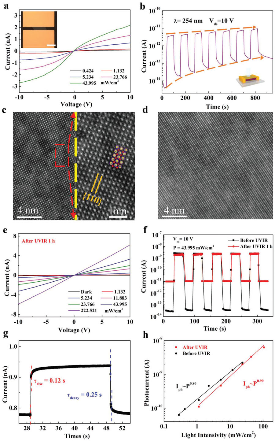 |
| Figure 2. Photodetectors based on 2D BiOI crystals. (a) I-V curves of the BiOI device illuminated by 473 nm laser with different light intensities. Inset shows the OM image of the corresponding device. Scale bar, 20 µm. (b) I-t curve of the device under 254 nm light. (c) ADF-STEM image of a pristine BiOI nanosheet. The right half shows a magnified STEM image and the position of Bi atom columns and O atom columns were marked by yellow and read circles, respectively. (d) ADF-STEM image of the BiOI nanosheet after UVIR for 20mins. (e) I-V curves of the BiOI device illuminated by different light intensities of 473 nm laser after UVIR. (f) I-t curves before (black) and after (red) UVIR under the same light intensity of 473 nm laser. (g) Response time for rise time of 0.12 s and decay time of 0.25 s. (h) Photocurrent as a function of 473 nm light intensities before (black) and after (red) UVIR.(Image: Reprinted with permission by Wiley-VCH Verlag) (click on image to enlarge) |
| These results have been published in Advanced Functional Materials ("Synthesis of large area atomically thin BiOI crystals with highly sensitive and controllable photodetection"). This work describes a novel method for preparing large-area, atomic-scale thin 2D BiOI crystals. |
| Additionally, this is the first attempt to fabricate and study photodetectors based on 2D BiOI. These findings are of scientific importance to understand the growth mechanism of 2D BiOI crystals and also of technical significance to further explore the potential applications of BiOI semiconductors in optoelectronic devices. |
|
By Xuming Zou
|

Become a Spotlight guest author! Join our large and growing group of guest contributors. Have you just published a scientific paper or have other exciting developments to share with the nanotechnology community? Here is how to publish on nanowerk.com. |
