| Nov 07, 2019 |
Paving the way for inorganic perovskites' use in high-performance electronic applications |
| (Nanowerk Spotlight) Hybrid organic-inorganic halide perovskite has attracted tremendous attention as an exceptional new class of semiconductors for solar harvesting, light emission, lasing and thin-film electronics. |
| However, the toxicity of lead devices and lead manufacturing combined with the instability of organic components have been two key barriers to widespread application. Tin-based inorganic halide perovskites, such as CsSnX3 (X = Cl, Br, and I), have been considered promising substitutes for their lead analogues. |
| "Compared with lead halide perovskites, the crystalline thin-film fabrication of inorganic and lead-free perovskites has been more challenging and has limited development in high-performance photovoltaics and optoelectronics due to a lower defect tolerance," says Richard Lunt, a professor at Department of Chemical Engineering and Materials Science, Michigan State University. "We think that this type of material has enormous potential and epitaxy is the key to achieving high quality crystalline thin-film growth and enhancing the optoelectronic properties of the devices based on them." |
| With the previous success of achieving single domain epitaxy of CsSnBr3 from room temperate vapor phase growth, the collaborated research team from Michigan State University and University of Michigan further demonstrates the singe crystalline growth of a new stabilized epitaxial tetragonal phase. |
| This work is featured as the recent front cover of ACS Applied Materials & Interfaces ("Epitaxial Stabilization of Tetragonal Cesium Tin Iodide"). |
| "Finding the substrate that provides the least lattice misfit is the key to achieving good epitaxial growth," says Pei Chen, a PhD student in Lunt's lab who conducted the growth studies in this work. "Alkali halide substrates provide an ideal range of lattice constants closely matched to those of the halide perovskites with suitable wettability and congruent ionic bonding." |
| Through room temperature epitaxy, a new stabilized epitaxial tetragonal phase for CsSnI3 is achieved, which is a phase slightly distorted from the high temperature cubic phase. |
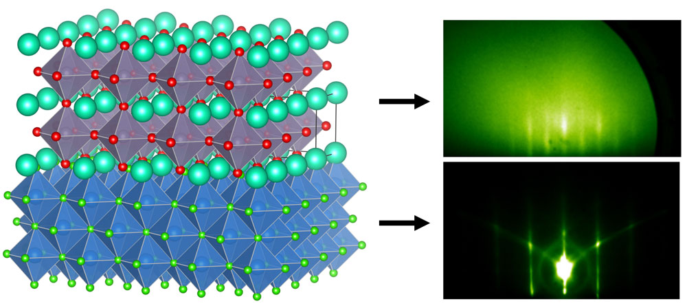 |
| Figure 1. Epitaxy: Schematic of the epitaxial structure of the CsSnI3 film on single-crystal potassium chloride substrate (left) and reflection high-energy electron diffraction (RHEED) patterns (right). (Image: Molecular and Organic Exitonics Lab, MSU) (click on image to enlarge) |
| Using in situ diffraction monitoring, the researchers built a high-quality quantum well structure and observed a photoluminescence shift by adjusting well thickness. |
| The team also incorporated the epitaxial film into a lateral photodetector application showing good photoresponse. "We are aiming at low-cost and low-toxicity devices," says Lili Wang, a research associate in Lunt’s lab who led this project. "This demonstration suggests exciting potential for all inorganic epaxial halide perovskite-based devices." |
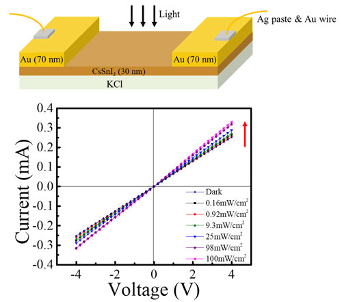 |
| Figure 2. Photovoltaic Application: Architecture (top) and current-voltage characteristics (bottom) of single crystalline CsSnI3 thin-film-based photodetector. (Image: Molecular and Organic Exitonics Lab, MSU) |
| "Our work provides insight into the control over phase and ordering during halide perovskite epitaxial growth and expands the selection of photoactive materials for growing epitaxial halide perovskites that can be exploited in high-performance electronic applications," Lunt concludes. |
|
Provided as a Nanowerk exclusive by Michigan State University
|

Become a Spotlight guest author! Join our large and growing group of guest contributors. Have you just published a scientific paper or have other exciting developments to share with the nanotechnology community? Here is how to publish on nanowerk.com. |
