| Feb 20, 2020 |
Programmable doping of 2D materials by nonvolatile ferroelectric domains |
| (Nanowerk Spotlight) Two-dimensional (2D) materials could offer new building blocks for future technologies, but this requires approaches to control the carrier type in 2D semiconductors. A number of pioneering works have demonstrated different methods to program the carrier type in 2D materials, such as electrostatic doping, chemical doping, ion implantation, charge transfer, and annealing control. |
| Recently, a team of researchers from Shanghai Institute of Technical Physics of the Chinese Academy of Sciences have developed a technique to dope 2D materials for redefinable nanoelectronics using nonvolatile ferroelectric domains. |
| "In previous work, ferroelectric materials were used to tune the transport properties and band structure of different 2D materials," says Professor Jianlu Wang, senior author of a recent paper in Nature Electronics ("Programmable transition metal dichalcogenide homojunctions controlled by nonvolatile ferroelectric domains"). Piezoresponse force microscopy (PFM) is a variation of atomic force microscopy (AFM) that allows patterning and manipulation of ferroelectric domains. One day, when we were performing PFM tests as usual, we came up with a new idea." |
| "What would happen if we replace the bottom electrode with a 2D material?" he continues. "In this condition, PFM is not a technique to characterize ferroelectric materials, but a method to control the properties of 2D materials. The atomically-thin nature of 2D materials, together with atomic precision of PFM, makes it a great prospect in nano-device applications." |
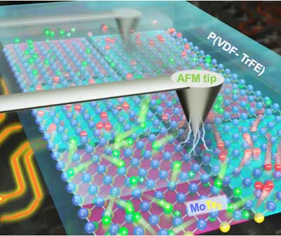 |
| A MoTe2 lateral p-n-p-n homojunction tuned using probe-controlled ferroelectric domains. Electrons/holes were injected into the channel when the ferroelectric polymer-P(VDF-TrFE) was polarized down/up. (Image: Shanghai Institute of Technical Physics, CAS) |
| The realization of p- and n-doping is essential for the fabrication of 2D semiconductor devices with advanced functionality. In this work, the researchers demonstrated a ferroelectric domain patterning method to dope 2D materials. |
| The ferroelectric film was polarized up when the conductive probe was scanning over the surface of the ferroelectric film with a negative voltage. The ferroelectric polarization takes advantage of the nonvolatility of electrostatic fields at the interface to dope the MoTe2 underneath. Holes were injected into the MoTe2 channel to screen the polarization field, thus a p-doped MoTe2 was created. |
| Similarly, an n-doped MoTe2 channel could be obtained when the ferroelectric film was polarized down by using a positive scanning voltage. |
| The ferroelectric domain patterns can be written free of the restrictions of a metal electrode and edited arbitrarily based on the PFM scanning technique. Furthermore, the ferroelectric polarization is non-volatile, which can be changed by external voltage pulse. This means the written ferroelectric domain pattern can be erased and rewritten to fabricate new functional devices. |
| Unlike conventional electrostatic doping, the ferroelectric field formed by the orderly arrangement of the dipoles at the interface is non-volatile. The polarization direction of ferroelectric materials can be controlled by the voltage applied to the PFM tips, which act like a gate electrode in the conventional transistor. |
| This doping method has its unique charms. Compared with traditional transistors with fixed gate electrodes, the PFM tip can move freely, which frees the ferroelectric domain patterns of the restrictions of the metal electrode and edited arbitrarily. |
| Based on this tip scanning technique, the team fabricated electronic and optoelectronic devices, such as MoTe2 p-n, n-p, p-p, n-n homojunctions, and an electrical writing and optical reading memory devices. |
| They also explored a type of quasi-non-volatile memory with the assistance of the ferroelectric domain pattern method with Peng Zhou?s research group at Fudan University, which demonstrates a refresh time of 100 s and a write/erase speed of 10 µs. |
| According to Jianlu Wang, ?The next step would be an improvement of the ferroelectric field by reducing the depolarization field to optimize the stability and durability of the devices.? |
|
Source: Provided as a Nanowerk exclusive by Shanghai Institute of Technical Physics of the Chinese Academy of Sciences
|

Become a Spotlight guest author! Join our large and growing group of guest contributors. Have you just published a scientific paper or have other exciting developments to share with the nanotechnology community? Here is how to publish on nanowerk.com. |
