| Apr 17, 2020 |
Enhanced light absorption in silicon by phase engineering |
| (Nanowerk Spotlight) Silicon (Si), which crystallizes in the diamond cubic (dc) lattice at room temperature and pressure, is known to exhibit several polymorphs at high-pressures. The dc-Si is a celebrated material for current electronics and solar cell applications. Researchers are always looking for new ways to improve the optoelectronic properties of Si to design low-cost and light-weight solar cells. |
| In 2008, researchers from the University of California at Berkeley performed first-principles calculations and showed that the rhombohedral phase (R8) of silicon, which is stable at ambient temperature, has interesting optoelectronic properties suitable for a solar absorber application (Physical Review B, "Ab initio study of the optical properties of Si-XII"). |
| Since then, no experimental studies have been published in utilizing the R8-Si for any application. However, researchers have thoroughly investigated the properties of indentation and diamond anvil cell- assisted phase engineered R8-Si using in-situ and ex-situ advanced characterization methods. Further, there is no success yet on the direct growth or synthesis of either thin-film or single crystal forms of R8-Si and its usage for solar cell applications. |
| New work led by Dr. Abhay Sagade and Dr. Kiran Mangalampalli from the SRM Institute of Science and Technology, Kattankulathur, Chennai, India, shows the formation of large-area R8-Si within the top n-layer of the p-n junction Si solar cell using spherical nanoindentation, and experimentally measured optical properties of R8-Si to demonstrate ten times enhancement in its photocurrent density. |
| The researchers published their results in the journal Scripta Materallia ("On the indentation-assisted phase engineered Si for solar applications"). |
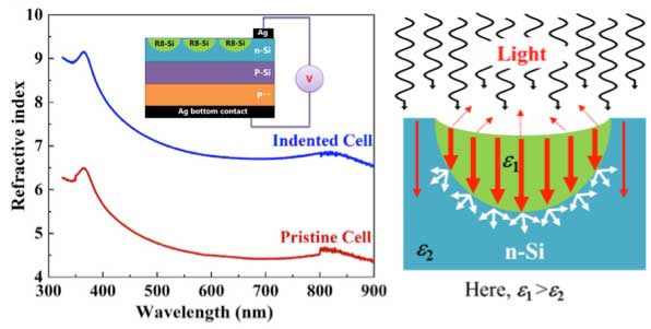 |
| Left: Variation of the refractive index of dc-Si (pristine cell) and R8-Si (indented cell). Right: Schematic of a cross-sectional view of single indentation induced R8-Si (green) in dc-Si (blue). On illumination, the light absorption ability of R8-Si is more (thick red arrows) compared to dc-Si (thin red arrows). Here, ε stands for dielectric function. (click on image to enlarge) |
| The key aspects of the study are: 1) the absorbing layer of R8-Si is made out of the same material (top n-layer of dc-Si); 2) as the interface between the R8-Si and the active layer (n-Si) is contamination-free, the series resistance of the cell can be minimized; and 3) since the R8-Si absorbs a greater fraction of the incident light, the thickness (~1-10 µm) can be well-controlled by optimizing the indentation conditions and therefore, the weight of the cell can be further reduced. |
| The researchers have shown that how the contribution of light-scattering effects are minimal and R8-Si plays an important role in absorbing the light. |
| "We provide the first experimental evidence of the theoretical results predicted in 2008 and our results highlight the potential of such phase engineered R8-Si integration into the dc-Si p-n junction solar cells which pave a path in realizing low-cost, light-weight and high-efficiency solar cells," conclude Sagade and Kiran. |
|
Provided by SRM Institute of Science and Technology, Kattankulathur, Chennai as a Nanowerk exclusive
|

Become a Spotlight guest author! Join our large and growing group of guest contributors. Have you just published a scientific paper or have other exciting developments to share with the nanotechnology community? Here is how to publish on nanowerk.com. |
