| Jul 23, 2020 |
Drawing photodetectors on paper |
| (Nanowerk Spotlight) A big chunk of the price tag of electronic components is due to the cost of silicon wafer substrates. Although silicon is a highly abundant and cheap element, the transformation and processing of the raw material into high quality silicon wafers results very costly (See: “Why Are Computer Chips So Expensive?”). |
| The societal, industrial and technological demands of biodegradable ultra-low-cost electronic components has spurred the quests towards lower cost substrates and it has naturally motivated a surge of works on paper-based electronics (read more: “Paper electronics is successful: Where next?” and “Printing solar cells and batteries on paper”). |
| Despite the promises of paper-based electronics, there are several challenges to be solved. One of the major challenges is that the rough, fiber-based, structure of paper makes it impossible to fabricate devices using conventional lithographic techniques. |
| Researchers at the Materials Science Institute of Madrid, part of the Consejo Superior de Investigaciones Científicas (CSIC, the Spanish National Research Council), and Delft University of Technology have fabricated photodetectors on paper by mimicking the action of drawing/writing with a pencil on standard paper. |
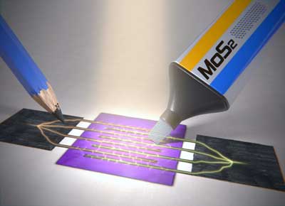 |
| Artistic representation of the MoS2 based photodetector, drawn on paper by rubbing a MoS2 crystal against standard copier paper. (Image: Enrique Sahagún, SCIXEL) |
| “When we draw with pencil on paper we exploit the fact that the surface of paper is very rough (fibrous), thus by rubbing a layered material (like the graphite in the pencil lead) the abrasion forces are strong enough to cleave the layered material yielding a network of interconnected patches” explains Andres Castellanos-Gomez, Tenured Scientist at the Materials Science Institute of Madrid (CSIC). |
| The results, published in Nanoscale (“MoS2-on-paper optoelectronics: drawing photodetectors with van der Waals semiconductors beyond graphite”) emphasize that this process can be employed with other layered materials like the semiconducting molybdenum disulfide (MoS2) to fabricate electronic devices on paper: “There are many layered materials (so called van der Waals materials) that have similar mechanical properties to graphite and thus are susceptible of being cleaved upon mechanical rubbing against paper substrates”. |
| The researchers deposited films of a semiconducting layered material (MoS2) on standard copier paper finding that the films were composed by a densely packed network of platelets with a good electrical conduction. |
| These films were applied in photodetector devices finding good responsivities and a broad spectral bandwidth. The performance of the photodetectors even allowed to build a rudimentary camera using a paper-supported photodetector as imaging sensor. |
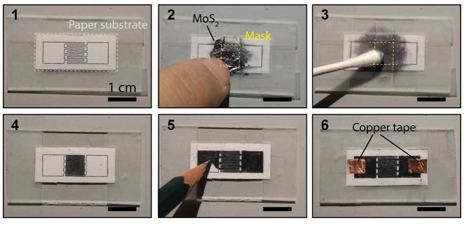 |
| Different steps for the fabrication of paper-supported MoS2 photodetectors. (1) The outline of the device is printed on paper with a standard office laser printer. (2) The channel area is masked with adhesive tape and a MoS2 single crystal is rubbed against the unmasked channel area. (3) A cotton-swab is used to blur the deposited MoS2 material to achieve an homogeneous coating. (4) The mask is removed. (5) Graphite electrodes are drawn following the printed outline. (6) The final device. (Reprinted with permission from Royal Society of Chemistry) (click on image to enlarge) |
| “At the beginning we were fairly surprised with the good performance of these devices but we now understand that the fully dry mechanical deposition method yields good interconnects with a very intimate contact between the deposited platelets and without presence of foreign chemical species as it can happen with inkjet printing strategies,” he adds. |
| The authors foresee that these results constitute the beginning of a new line of research for scientists working on 2D materials (see also: Nature, "Heterostructures formed through abraded van der Waals materials"). |
| “This is a very exciting avenue, we can now translate most of the knowledge that we gained in the last years on these layered materials at the nanoscale to real-life devices”, Castellanos-Gomez concludes. |
|
Provided by Instituto de Ciencia de Materiales de Madrid
|

Become a Spotlight guest author! Join our large and growing group of guest contributors. Have you just published a scientific paper or have other exciting developments to share with the nanotechnology community? Here is how to publish on nanowerk.com. |
