| Feb 08, 2021 |
Femtosecond laser converts metallic to semiconducting carbon nanotube |
| (Nanowerk Spotlight) Contemporary microtechnology (which contains elements of nanoelectronics, as feature sizes of transistors often are less than 10 nm) is still based on conventional methods of mask-based lithography. In this process, the electrical properties of transistor channels are tuned by chemical modification processes, providing the fabrication of billions of transistors per single process. |
| Nevertheless, when we turn to nanomaterials such as graphene and carbon nanotubes, the traditional methods of lithography can result in many impurities, which are drastically altering these materials' properties. New maskless methods are therefore highly desirable for the processing of novel materials. |
| Among various direct writing methods like electron and ion beam lithography, laser processing has become a fast growing processing tool in different application areas. Novel technologies based on nonlinear effects of irradiation provide photochemical processing and 3D printing of different materials ranging from metals to biological polymers. |
| This technology is supported by both ultrafast scanning system development (that can speed up processing to kilometers per seconds) and focusing techniques below the diffraction limit (e.g. STED lithography). Yet the demonstration of functional electronic device development based on fully optical methods is still challenging. |
| A team of researchers from Russia and Spain has developed a method for fast and accurate local tuning of the optoelectronic properties of single-walled carbon nanotubes by making use of ultrafast-pulsed lasers. The method is based on localized two-photon oxidation of carbon nanotubes when the laser irradiates with energies far below the ablation threshold. At such low energies the nonlinear photochemical interaction of femtosecond laser and carbon atomic lattice prevent thermal effects. |
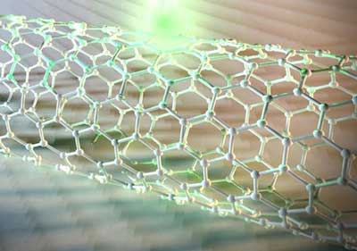 |
| Illustration of local two-photon modification of a single-walled carbon nanotube by femtosecond laser. (Image: Ivan Bobrinetskiy) |
| This low-cost, facile, and versatile direct patterning technique based on femtosecond (10-15 seconds) laser processing is applied to individual single-walled carbon nanotube transistors to convert quasimetallic to semiconducting nanotubes by grafting oxygen species and form a planar junction between pristine and modified parts of a nanotube to detect ultralow light intensities in a broadband light range. |
| The process requires only a single laser pulse, which makes it unprecedentedly fast. |
| The research team has reported their findings in Advanced Electronics Materials ("Individual SWCNT Transistor with Photosensitive Planar Junction Induced by Two-Photon Oxidation"). |
| To demonstrate the performance of this method, the researchers created a single-walled carbon nanotube (SWCNT) detector, which provides high sensitivity to visible optical radiation in combination with high-speed response. The fabricated planar junction in the nanotube changes its conductivity under optical radiation and makes it possible to detect a single pulse with a duration of 300 femtoseconds with a power down to 0.2 mW/cm2, which corresponds to the power of optical fiber systems in modern telecommunication. |
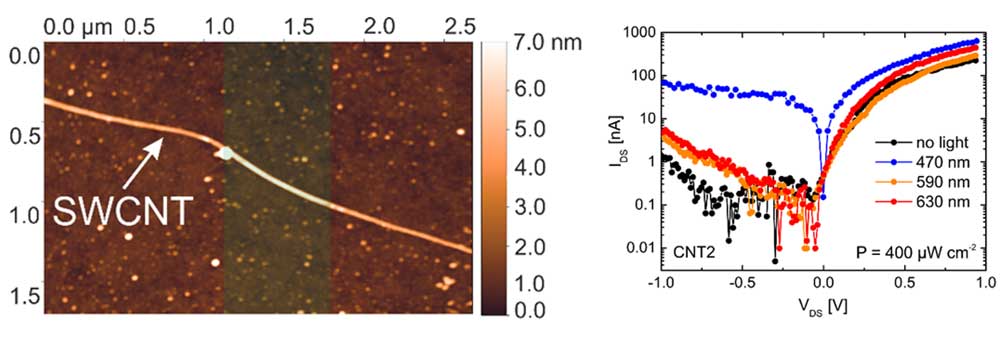 |
| Single-walled carbon nanotube with fs-laser modified central region and electrical characteristic of formed junction in carbon nanotubes under different light wavelengths. (Reprinted with permission from Wiley-VCH Verlag) (click on image to enlarge) |
| The main benefit of a purely optical technology is the possibility of future miniaturization and its integration on a chip compatible with conventional microelectronics manufacturing technologies, paving the way for on-site customized tuning of the optical and electronic properties of photonic devices. |
| A Nanowerk exclusive provided by National Research University of Electronic Technology |

Become a Spotlight guest author! Join our large and growing group of guest contributors. Have you just published a scientific paper or have other exciting developments to share with the nanotechnology community? Here is how to publish on nanowerk.com. |
