| Mar 24, 2021 |
New theory unveils obscure nonvolatile resistive switching in 2D materials |
| (Nanowerk Spotlight) Computers play a key role in our day-to-day life. They are used in home, business, educational institutions, research organizations, industries etc. These machines are designed based on von Neumann architecture, where the central processing and memory units are physically separated but connected with a bus (a communication system) that controls the in-between data transfer. |
| This architecture has served the purpose so far until we embarked on the era of artificial intelligence (AI). Since an instruction fetch and a data operation cannot occur at the same time in shared a common bus, the limitations of mordern computers in executing deep-learning algorithms are being exposed. This limitation is known as ‘von Neumann bottleneck’. |
| It is worth noting that in our brain, which is also a type of computing machine, the data processing units and memory cannot be physically isolated. Our brain can execute very complex tasks much more efficiently than any computer in this world. Such neuromorphic computing demands processing units to be embedded in memory, which is known as in-memory computing. |
| This new computing paradigm demands a very different kind of memory technology than our commercial DRAM (dynamic random-access memory), which consists of one transistor and one capacitor. |
| Nonvolatile resistive memory (NVRM), often called a 'memristor', is one such emerging technology that offers the possibility of in-memory computation and thus holds promise to overcome the von Neumann bottleneck. NVRM is a two-terminal device but, unlike an ordinary resistor, it exhibits hysteresis in input-output characteristics and thus can be also be used as memory. |
| Basically, with the application of an external electrical signal, the resistance changes between two states – high and low – and this change is nonvolatile (which means the device can preserve the state even when the signal is withdrawn). Several recent reports show that a highly dense crossbar array of memristors can outperform state-of-the-art computers in executing complex AI algorithms. |
 |
| Proposed mechanism of resistive switching in monolayer molybdenum sulphide: the interlayer movement of sulphur atom creates states on Fermi level position and induce conductive path between two electrodes. Such movement can be controlled by external electric field and the state could be preserved once the electric field is withdrawn (Image: Prof. Santanu Mahapatra, Indian Institute of Science, Bangalore) |
| A memristor is generally built upon MIM (metal-insulator-metal) architecture. While the oxide based memristor technology is nearing commercialization, with the emergence of various two-dimensional (2D) materials, the recent past has witnessed a surge of experimental demonstrations where atomically thin layers are used as insulators. |
| These 2D memristors can overcome the vertical scaling obstacle of oxide-based devices and offer highly dense, fast, and ultra-low power technology solutions. Despite their technological advancements, the underlying physics behind the ultra-fast resistive switching (RS) in these atomically thin devices is not yet well understood. |
| The conventional oxide-based memristors work under well-established ‘filament formation and rupture’ theory. However, this is not applicable here since the remarkable RS is also observed in 2D memristors having chemically passive electrodes like graphene. |
| In our recent work, which is published in npj 2D Materials and Applications ("Theory of nonvolatile resistive switching in monolayer molybdenum disulfide with passive electrodes"), we investigate the origin of resistive switching in a monolayer molybdenum sulfide (MoS2) based memristor, also known as atomristor. |
| We use reactive molecular dynamics simulation, which can model chemical reactions such as bond breaking and formation with an accuracy close to that of ab initio simulations with a much lower computational expense. |
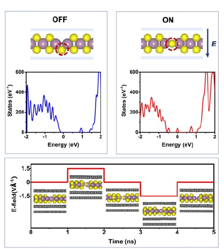
| A monolayer MoS2 flake, sandwiched between two electrodes, normally offers a very high resistance since the hexagonal phase of MoS2 is semiconducting in nature even in the presence of sulfur vacancy defects. |
| We discover that with the application of a suitable electric field at the vacancy positions, the sulfur atom from the other plane 'pops' and gets arrested in the plane of the molybdenum atoms. Rigorous first principles-based calculations surprisingly reveal localized metallic states and stronger chemical bonding for this new atomic arrangement. |
| This metastable state with popped sulphur atom acts as a ‘virtual’ filament and creates a conductive bridge between two electrodes and turns the device ‘ON’. The stronger chemical bonding holds the sulphur atom in this metastable state when the electric field is withdrawn and thus creates a nonvolatile memory effect. |
| We further notice that localized Joule heating plays a crucial role in restoring the popped sulfur atom to its original position (RESET process), which is also observed in experiments. |
| Our theory suggests that such resistive switching is an intrinsic property of a vacancy-inhabited two-dimensional materials and may not depend on the physio-chemical interactions with the electrodes. It explains almost all the observations made in experiments including both bipolar and unipolar switching. |
| This atomistic insight provided in our work opens up the possibility for precise defect engineering in 2D materials for the realization of ReRAM based ultra-low-power neuromorphic circuits. |
| Provided by Nano Scale Device Research Laboratory, Department of Electronic Systems Engineering, Indian Institute of Science Bangalore as a Nanowerk exclusive |

Become a Spotlight guest author! Join our large and growing group of guest contributors. Have you just published a scientific paper or have other exciting developments to share with the nanotechnology community? Here is how to publish on nanowerk.com. |
