| Apr 22, 2021 |
Steering waves deep into a forbidden gap |
| (Nanowerk Spotlight) The propagation of light can be radically controlled with tailor-made nanostructures, called photonic crystals. The main feature of such crystals is a forbidden gap: waves with colors within a forbidden range travel only a limited distance – called Bragg length – before being reflected due to Bragg interference. Once a crystal is fabricated its properties are fixed including the Bragg length. |
| Recently, a team of scientists from the University of Twente (Netherlands), the University of Iowa (USA) and the University of Copenhagen (Denmark) has discovered a method to tunably steer light deep into photonic crystals, to depths well beyond the Bragg length. By spatially shaping the incident waves, the energy density of the light is enhanced at tunable distances deep inside the crystals. |
| The team takes advantage of new wave forms that are induced by unavoidable fabrication deviations of the nanostructures from their design. The results are relevant to applications such as efficient miniature light sources and tiny on-chip lasers, robust qubits, and 3D photonic integrated circuits that shuttle information encoded as photons instead of electrical currents. |
| The team's paper will soon appear in the world's leading physics journal Physical Review Letters. A preprint is available on the Cornell preprint server Arxiv ("Spatially shaping waves to penetrate deep inside a forbidden gap") |
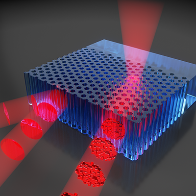 |
| Figure 1. Left: Light propagation inside a photonic crystal is forbidden by a propagation gap. Hence common plane waves are reflected and hardly penetrate into the crystal. Right: By shaping the incident waves, one steers the waves deep into the crystal, thereby enabling the focusing of light at any desirable depth inside the otherwise forbidden gap. (Image: COPS, University of Twente) |
| In our daily life, we see that mirrors and reflectors serve to control how light waves propagate from one place to another one (target). While conventional mirrors like those in bathrooms are made of metals that absorb a sizable fraction of the light, scientists have found over the years that nanostructures allow to realize near-perfect mirrors. Such nanostructures are called photonic crystals and can be realized by etching nanopores – each with a diameter one-thousandth that of a human hair – in a periodic arrangement. |
| Photonic crystals can be made to perfectly reflect a chosen color band, thereby realizing a forbidden band for light. If an atom that emits such a color in the forbidden band is placed inside the crystal, it stops emitting as light with these colors cannot exist within the crystal. |
| This control on the emission properties has led to a wide variety of applications such as, e.g., optical memory to store information encoded as light, and nonlinear processors for quantum computing. |
Background |
| Photonic crystals are attracting considerable technological attention due to their novel functionalities. Photonic crystals consist of periodically ordered materials that have a spacing of the order of the wavelength of light. Due to the periodic order, color ranges emerge for which light is forbidden to propagate into or inside the crystal due to Bragg interference. |
| As a result, the light only penetrates to a shallow depth, called the Bragg length (see Fig. 1, top), in honor of father and son William H. and William L. Bragg who jointly received the Physics Nobel Prize for diffraction of X-ray waves. In specific photonic crystals, a frequency range appears for which light is forbidden to propagate in any direction, called the photonic band gap. |
| The photonic band gap was predicted in 1987 by American scientists Eli Yablonovitch and Sajeev John and is rapidly being integrated into light sources and lasers, efficient solar cells, invisibility cloaks, trapped light in extremely small volumes, and information-processing with light. |
| However, all these applications are static, i.e., the crystals and the light transport is fixed; novel functionality could be obtained if light could be controllably sent anywhere inside a photonic crystal. This steering of light inside the crystal circumvents a forbidden gap and improves the scalability for the aforementioned applications. |
| The researchers now take a major step by observing light deep inside photonic crystals upon programmable steering. Hence, the light can be directed to any location. |
| The researchers fabricated high-quality photonic crystals from silicon, using semiconductor industry (CMOS) compatible methods, which make them suitable for on-chip integration. The crystals consist of tiny pores (thousand times thinner than a human hair) etched in silicon using an etch mask. The crystals exhibit excellent powerful gaps in the telecom wavelength range. |
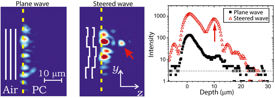 |
| Figure 2: Steering of telecom light inside a silicon photonic crystal. The false color camera images show that light incident with plane wave front (left panel) does not enter inside the crystal, while an intense spot marked by the red arrow was observed at a depth of 10 µm inside the crystal upon steering (middle panel). Right panel: The depth-dependent intensity of light inside the crystal extracted from the false color images shows a 100x intensity enhancement with steering at the target location. (Image courtesy of the researchers) (click on image to enlarge) |
Observations |
| In their studies, the team first directed unstructured, plane, waves onto the crystals. They viewed the light that leaks through the top surface, which represents the energy density of light at any given position inside the crystal. The camera images show that light hardly penetrates into the crystal (see Fig. 2), as expected for good quality crystals and confirmed by 95% reflectivity of the incident light. |
| Next, the authors chose an arbitrary position inside the crystal where light should be delivered. To this end, the team shaped the incident wavefronts using a spatial light modulator, which is a central component of projection devices like beamers, projection televisions. By programming the incident wavefront using the spatial light modulator, the authors realized a bright spot deep inside the crystal, see Fig. 2. |
| As shown in a cross-section (Fig. 2, right) the authors observed hundred-fold enhancement of light at the chosen location that is 5 Bragg lengths deep. For comparison, if the incident light would not be shaped, the intensity at the chosen depth would be severely decreased by a hundred to a thousand times. |
| The method works by utilizing the unintentional disorder (few nanometers) that occurs in all nanofabrication processes. The addition of this small amount of disorder causes a small fraction of waves to randomly scatter into the crystal instead of being reflected. By wavefront shaping the incident light, the authors ensure that the light selectively coupled to these wave channels that penetrate deep into the crystal. |
| Moreover, by programming the wavefront correctly, these waves can be interfered such that the intensity concentrates into a single location deep inside the crystal as highlighted by their observations. |
The team |
| The research has been performed by prof. Ravitej Uppu from the Physics Department of the University of Iowa, previously with the Complex Photonic Systems (COPS) chair in the MESA+ Institute for Nanotechnology at University of Twente, and at the Niels Bohr Institute in Denmark, Manashee Adhikary MSc, Cornelis Harteveld, and prof. Willem Vos from the Complex Photonic Systems (COPS) chair in the MESA+ Institute for Nanotechnology at University of Twente. |
| Further information can be obtained from: |
| Prof. Ravitej Uppu, email: [email protected], Phone +1 319 467 3201 |
| Prof. Willem Vos, email: [email protected], phone +31 (0) 53 489 5388 or +31 (0)6 47386517 (mobile). |
| Provided by the researchers |

Become a Spotlight guest author! Join our large and growing group of guest contributors. Have you just published a scientific paper or have other exciting developments to share with the nanotechnology community? Here is how to publish on nanowerk.com. |
