| Sep 04, 2021 |
2D Materials cut sharper |
| (Nanowerk Spotlight) Researchers from the Technical University of Denmark have taken the art of patterning nanomaterials to the next level (ACS Applied Materials and Interfaces, "Super-Resolution Nanolithography of Two-Dimensional Materials by Anisotropic Etching"). |
| Precise patterning of 2D materials is a route to computation and storage using 2D materials, which can deliver potentially better performance and much lower power consumption compared to the technology of today. |
| One of the greatest discoveries within physics and material technology for quite some years are the two-dimensional materials such as graphene – stronger, smoother, lighter and better at conducting heat and electricity than any other known material. |
| Their most unique feature is perhaps their programmability. By creating fine patterns in these materials, we can change their properties dramatically, and perhaps create exactly what we need. This was demonstrated in 2018 where American researchers showed that graphene can be turned into a superconductor, by exploiting the graphene’s own crystal lattice to create super-lattices – periodic patterns. |
| At DTU the researchers have for more than a decade worked on improving the state of the art in patterning 2D materials, using sophisticated lithography machines in the 1500 m2 cleanroom facility. The electron beam lithography system in DTU Nanolab can write details down to 10 nanometers. |
| Computer calculations can predict exactly the shape and size of patterns in the graphene to create new types of electronics, which exploit not just the charge of the electron, but also quantum properties such as spin or valley degrees of freedom, which could lead to high speed calculations with far smaller power consumption. |
| These calculations, however, asks for higher resolution than even the best lithography systems can deliver: atomic resolution. |
| “If we really want to unlock the treasure chest for future quantum electronics, we need to go below 10 nanometer, and approach the atomic scale. We showed in 2019 that circular holes placed with a just 12 nanometer spacing turns the semimetallic graphene into a semiconductor. Now we know how to create not just circular holes, but other shapes such as triangles, with nanometer sharp corners. Or any other shape,"explains Peter Bøggild, professor and group leader at DTU Physics. |
| "Such patterns can be used to sort electrons based on their spin, and create essential components for spintronics or valleytronics,"he continues. "The technique also works on other 2D materials, and we will use these super small structures to create very compact, electrically tunable metalenses which can be used for high speed communication and biotechnology for example." |
| The research was led by postdoc Lene Gammelgaard, who herself graduated as an engineer from DTU in 2013, and has since played a key role in the experimental exploration of 2D materials at DTU. |
| “The trick is to place the nanomaterial hexagonal boron-nitride on top of the material you want to pattern, and then drill these holes with a very specific etching recipe," says Gammelgaard. “The etch process we developed over the past years, down-size patterns below the otherwise unbreakable limit electron beam lithography systems of ca. 10 nm. If we make a circular hole with a diameter of 20 nanometer, the hole in the graphene can be downsized to 10 nanometer. If we make a triangular hole, with the round holes coming from the lithography system, the downsizing will turn it into a smaller triangle, with self-sharpened corners. Usually patterns get more imperfect when you make them smaller. This is the opposite, and this allows us to recreate the structures the theoretical predictions tell us are optimal “ |
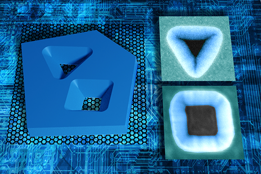 |
| Crystals of the material hexagonal boron nitride can be etched so that the pattern you draw at the top transforms into a smaller and razor-sharp version at the bottom. These perforations can be used as a shadow mask to draw components and circuits on the honey-comb material, graphene. This process enables a precision that is impossible with even the best lithographic techniques today. To the right are images of triangular and square holes taken with an electron microscope. (Image: DTU) |
| The other key person is a young student, Dorte Danielsen. She got interested in nanophysics after a 9th grade internship already in 2012, won a spot in the final of a national science competition for high school students in 2014, and pursued studies in Physics and Nanotechnology at DTU under a special program for elite students. |
| She explains that the mechanism behind the “super-resolution” structures, is still not well understood: “We have several possible explanations for this unexpected etching behavior, but there is still much we don’t understand. It is for sure an exciting and highly useful technique for us, and good news for thousands of researchers around the world who are trying to push the limits for two-dimensional nanoelectronics and nanophotonics.” |
| Dorte Danielsen will get an opportunity to continue the work on extremely sharp nanostructures within the project “METATUNE” supported by the Independent Research Fund Denmark, where the technology she helped develop, will be used to create and explore optical metalenses that can be tuned electrically. The research was funded by the Graphene Flagship. |
| Source: Provided by the Technical University of Denmark |

Become a Spotlight guest author! Join our large and growing group of guest contributors. Have you just published a scientific paper or have other exciting developments to share with the nanotechnology community? Here is how to publish on nanowerk.com. |
