| Jan 31, 2022 |
New technique paves the way for mass production of perovskite solar cells |
| (Nanowerk Spotlight) A collaborative team of scientists led by Professor Michael Grätzel at EPFL’s School of Basic Sciences have demonstrated a technique for producing perovskite photovoltaic materials on an industrial scale, which will reduce the cost and improve the performance of mass-produced perovskite solar cells. |
| The technique is low-cost, simple, energy-efficient, and should pave the way for creating perovskite solar cells. Perovskite is of interest for solar cells because it absorbs light very efficiently. This allows for the creation of lightweight, flexible solar cells that can be incorporated into a range of technologies, such as the windows of buildings or vehicles. |
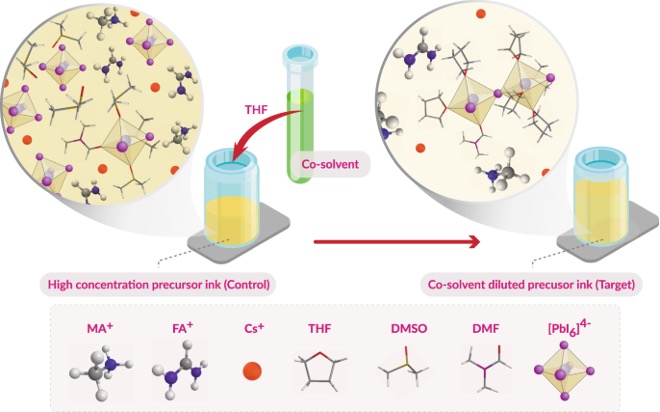 |
| Dilution of perovskite precursor inks by a co-solvent, top part of the panel: schematic illustration of the dilution process using tetrahydrofuran as a cosolvent. Bottom part of the panel: chemical compounds and their structure employed in the precursor solution. (Image: Hong Zhang) |
| "What we’ve done here is demonstrate that you can produce perovskite photovoltaics on larger substrates using spin coating by designing a co-solvent dilution strategy," says Grätzel, who is the lead co-corresponding author of a paper (Nature Communications, "A universal co-solvent dilution strategy enables facile and cost-effective fabrication of perovskite photovoltaics") on the work and a professor at École Polytechnique Fédérale de Lausanne. "The new technique also significantly reduces waste and, by extension, reduces toxic byproducts associated with manufacturing perovskite photovoltaics." |
| "Typically, there is a direct correlation between the thickness of the semiconductor film and the precursor ink concentration. Therefore, the high-efficiency perovskite solar cells require a high concentration (>1.4 M) of lead components to obtain thick and high-quality films. Encouragingly, our co-solvent dilution strategy breaks this general rule," says Hong Zhang, first-author on the paper. |
| "In the lab, researchers produce perovskite photovoltaic materials using a technique called spin coating, which creates a thin film of perovskite on a substrate – but only on a small scale,” says Aram Amassian, who is a professor at the North Carolina State University. "We’re talking about sample substrates that are only one or two centimeters square. However, people didn’t think it was possible to scale spin-coating up for manufacturing, using substrates that are tens of centimeters square. Instead, people have opted for a variety of other methods. But these other methods produce perovskite photovoltaics that don’t perform as well as the thin films made using spin coating and required significant research and development." |
| Historically, people thought spin coating could not be used to produce perovskite photovoltaics on industrial-scale substrates in a material-efficient way because of the nature of both spin coating and perovskites. |
| Spin coating involves placing a liquid on the surface of a substrate and then spinning the substrate, so that the liquid material spreads across the surface. However, when perovskite is applied using this technique, the solvents that keep the perovskite in a liquid state don’t evaporate quickly enough. This causes much of the perovskite to fly off the edges, meaning a lot of the perovskite material is wasted. It also results in irregular thickness of the perovskite on the surface, as well as some areas of the perovskite taking longer than others to dry. All of which is problematic from a manufacturing standpoint. |
| "The beauty of this technique is that many industries already use spin coating technologies to produce all sorts of products," says Aldo Di Carlo, professor at the University of Rome Tor Vergata. "Our work demonstrates that these existing technologies could be used to create perovskite solar cells. This could really accelerate the production and deployment of perovskite solar panels and cells." |
| Collaborators on the demonstration project are already using the new technique to produce modules that are tens of centimeters across with excellent uniformity and performance. |
| The work was done with support from the European Union’s Horizon 2020 research and innovation program (GRAPHENE Flagship Core 3 grant agreement No. 881603 as well as Espresso under agreement No. 764047), the Swiss National Science Foundation, the Italian Ministry of Economic Development, and the U.S. Office of Naval Research. |
| By Hong Zhang, Laboratory of Photonics and Interfaces, EPFL |

Become a Spotlight guest author! Join our large and growing group of guest contributors. Have you just published a scientific paper or have other exciting developments to share with the nanotechnology community? Here is how to publish on nanowerk.com. |
