| Aug 30, 2022 |
Scientists create a heterostructure of diversely behaving atomic layers within a single bulk material |
| (Nanowerk Spotlight) Researchers from the National Graphene Institute (NGI) of the University of Manchester (UK) have developed a new method to create interlayered bulk materials, comprising atomically-thin layers with highly diverse electronic properties – from insulating to superconducting. |
| The atomistic quantum mechanical simulations and electron microscopy imaging, performed at the NANOlab Center of Excellence of the University of Antwerp (Belgium), have illuminated the origin of this spectacularly diverse behavior between adjacent layers of a single material. |
| In 2004, the first atomically thin two-dimensional (2D) material was created: graphene, a single layer of carbon atoms. This feat yielded the scientists who achieved this, Andre Geim and Konstantin Novoselov from the University of Manchester, the Nobel Prize in Physics in 2010. This major breakthrough in physics and materials science has opened up a whole new research field on 2D materials and their technological applications. |
| Since that time, many new 2D materials have been discovered. The interactions between these materials are usually mediated by weak van der Waals forces. This facilitates controlled stacking of different layers into so-called van der Waals heterostructures, enabling the creation of new materials with properties tailored by design. |
| In a recent issue of the journal Nano Letters ("Alternating Superconducting and Charge Density Wave Monolayers within Bulk 6R-TaS2"), the researchers from the NGI and the NANOlab report on the synthesis and characterization of a novel van der Waals heterostructure of tantalum disulfide (TaS2, created not by selective stacking of 2D materials, but within a single bulk material. |
| This fabricated phase of TaS2 (denoted as 6R) consists of two alternating layers with distinct crystal structures and physical properties. At higher temperatures, both layer types are simply metallic. However, at low temperatures one turns into an insulator, while the other becomes superconducting. This implies that the former does not conduct electricity, yet the latter conducts perfectly (without any loss due to resistance). |
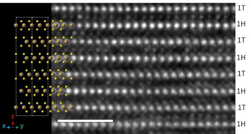 |
| Crystal structure of the 6R-phase of TaS2, consisting of alternating 1T and 1H monolayers, as obtained from scanning transmission electron microscopy (performed at the NANOlab Center of Excellence of the University of Antwerp). (Image: University of Antwerp) |
| To fully understand the origin of this unusual combination of highly diverse properties on the atomic scale, the material was theoretically and structurally investigated at the NANOlab. |
| The analysis using first-principles calculations and direct visualization at the atomic scale (see figure) has unequivocally proven that the coexistence of superconducting and insulating layers stems directly from the different atomic arrangements in the two-layer types. |
| Its alternating layered structure makes this material a true 2D superconductor in bulk form and opens a plethora of intriguing questions related to the effect of interlayer coupling on the superconducting behavior. |
| Moreover, it exemplifies an entirely new approach to create junctions of two superconductors separated by a thin insulating layer (so-called Josephson junctions), a key element of many modern technological applications, such as quantum sensors and qubit devices aimed at quantum computing. |
| Provided by the University of Antwerp |

Become a Spotlight guest author! Join our large and growing group of guest contributors. Have you just published a scientific paper or have other exciting developments to share with the nanotechnology community? Here is how to publish on nanowerk.com. |
