| Sep 02, 2022 |
Van der Waals infrared photodetectors based on 'optical' and 'electrical' combined manipulations |
| (Nanowerk Spotlight) Blackbody response is highly desired in two-dimensional (2D) infrared photodetectors, which determines their practical applications. State-of-the-art available blackbody response mid-wavelength infrared (MWIR) photodetectors are fabricated using materials such as HgCdTe, InSb and InAsSb. However, these photodetectors need to operate at cryogenic temperatures to minimize thermally generated dark current and noise, which not only increases the overall system size and cost but also limits their wide application. |
| Due to the quantum confinement effect and the strong light-matter interaction, 2D materials exhibit many novel features in the optoelectronic detection field. In particular, 2D materials without dangling bonds can reduce the noise generated by generation-recombination and avoid problems such as lattice mismatch. |
| However, limited by the thickness and complex defects of 2D materials, 2D photodetectors still suffer from problems such as low quantum efficiency and large dark current. With the expansion of detection wavelengths, the above problems of 2D infrared photodetectors will become more serious. |
| In new work (Advanced Materials, "Fully Depleted Self-Aligned Heterosandwiched Van Der Waals Photodetectors"), Fang Wang et al. have demonstrated fully depleted self-aligned van der Waals (vdW) photodetectors based on the MoS2-BP-MoS2 heterosandwiched structure. The structure solved the problems of low quantum efficiency and large dark current of 2D photodetectors in the MWIR by combined light field and electric field manipulation. |
| In terms of 'optical' manipulation, the top and bottom electrodes in the sandwiched structure form a microcavity, which can enhance the resonance of incident light, thereby improving the quantum efficiency of the photodetector. The optical absorption simulation results demonstrate that the constructed microcavity structure effectively realizes the enhanced photoresponse of the photodetector in the near-infrared band. |
| In terms of 'electrical' manipulation, the sandwich structure can completely deplete the carriers in the infrared absorption layer BP, thereby achieving effective suppression of dark current and efficient separation of photogenerated carriers. Additionally, the vertical stack structure and sandwich fully wrapped electrodes greatly shorten the transport distance of photogenerated carriers after separation, effectively reducing the recombination loss of photogenerated carriers in low-dimensional photodetection and improving the collection efficiency of photogenerated carriers. |
| In addition, a self-alignment process is also introduced into the structure, which almost eliminates the horizontal transport mode of photogenerated carriers in the 2D photodetector. At the same time, the longitudinal transmission distance in the built-in electric field is completely depleted by tens of nanometers, making the photodetector achieves a fast response speed. |
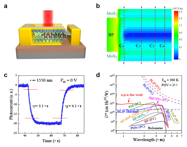 |
| Figure 1. a, Device structure of the MoS2-BP-MoS2 self-aligned heterosandwiched vdW photodetector. b, Simulated vertical potential distribution of the photodetector under zero bias. c, Rise and fall times of the photodetector at zero bias under a 1550 nm laser. d, Spectral detectivity comparison between the MoS2-BP-MoS2 vdW heterostructure photodetector, other MWIR photodetectors based on 2D materials, and commercially available infrared photodetectors. (Image courtesy of the researchers) |
| Based on the combined 'optical' & 'electrical' manipulation strategies, the photodetector finally achieved ultra-low noise of 10-25 A2 Hz-1, a blackbody peak responsivity of 0.77 A W???1, and a blackbody peak specific detectivity of 8.61 ?? 1010 cm Hz1/ 2 W???1 at room temperature. |
| This photodetector achieves the widest blackbody response spectrum of 2D infrared photodetectors reported so far. |
| Furthermore, the previously reported 2D photodetectors can only exhibit fast response in the visible or infrared band. Based on the unique electrical advantages of the fully depleted self-aligned structure, the photodetector achieve a fast response speed of 4 µs in both the visible and infrared bands. |
| These research results greatly expand the application prospects of 2D infrared photodetectors in the highly sensitive detection of weak signals at room temperature. |
| Provided by State Key Laboratory of Infrared Physics, Shanghai Institute of Technical Physics, Chinese Academy of Sciences |

Become a Spotlight guest author! Join our large and growing group of guest contributors. Have you just published a scientific paper or have other exciting developments to share with the nanotechnology community? Here is how to publish on nanowerk.com. |
