| Sep 05, 2022 |
A memristive forming strategy for lowering the contact resistances of two-dimensional semiconductors |
| (Nanowerk Spotlight) The silicon-based CMOS technology is fast approaching its physical limits, and the electronics industry is urgently calling for new techniques to keep the long-term development. Two-dimensional (2D) semiconductors, like transition-metal dichalcogenides (TMDs), have become a competitive alternative to traditional semiconducting materials in the post-Moore era, and caused worldwide interest. However, before they can be used in practical applications, some key obstacles must be resolved. One of them is the large electrical contact resistances at the metal-semiconductor interfaces. |
| The large contact resistances mainly come from two aspects: the high tunneling barrier caused by the wide van der Waals (vdW) gap between the 2D material and the metal electrode; the high Schottky barrier accompanied by strong Fermi level pinning at the metal-semiconductor interface. |
| Four strategies including edge contact, doping TMDs, phase engineering, and using special metals, have been developed to address this problem. However, they all have shortcomings. |
| The edge contact geometry is difficult to scale up. Stable, uniform, and non-destructive doping TMDs is still a challenge because of the ultrathin body feature. The high-conductivity materials after phase-engineering are usually thermodynamically unstable. And it is still needed to consider the energy difference between the metal work function and the semiconductor electron affinity when using special metals. Reducing the contact resistances with a feasible strategy, a stable performance, a wide generality no need considering the material type keeps an open question. |
| In a new work (Nano Letters, "Van der Waals Epitaxy and Photoresponse of Hexagonal Tellurium Nanoplates on Flexible Mica Sheets") coming out of Zhenxing Wang's group at the National Center for Nanoscience and Technology, the researchers have proposed a brand-new contact resistance lowering strategy of 2D semiconductors with a good feasibility, a wide generality and a high stability. |
 |
| Researchers successfully realize obvious contact resistances lowering of 2D semiconductors with a good feasibility, a wide generality and a high stability, through a memristive forming strategy. During forming, vacancies redistribute, conductive filaments form, the layers inside TMDs become more conducting to each other, and the Fermi level of TMDs is leveled to that of the contact metal. Finally, the total contact resistance of 2D semiconductors decreases.(© ACS) |
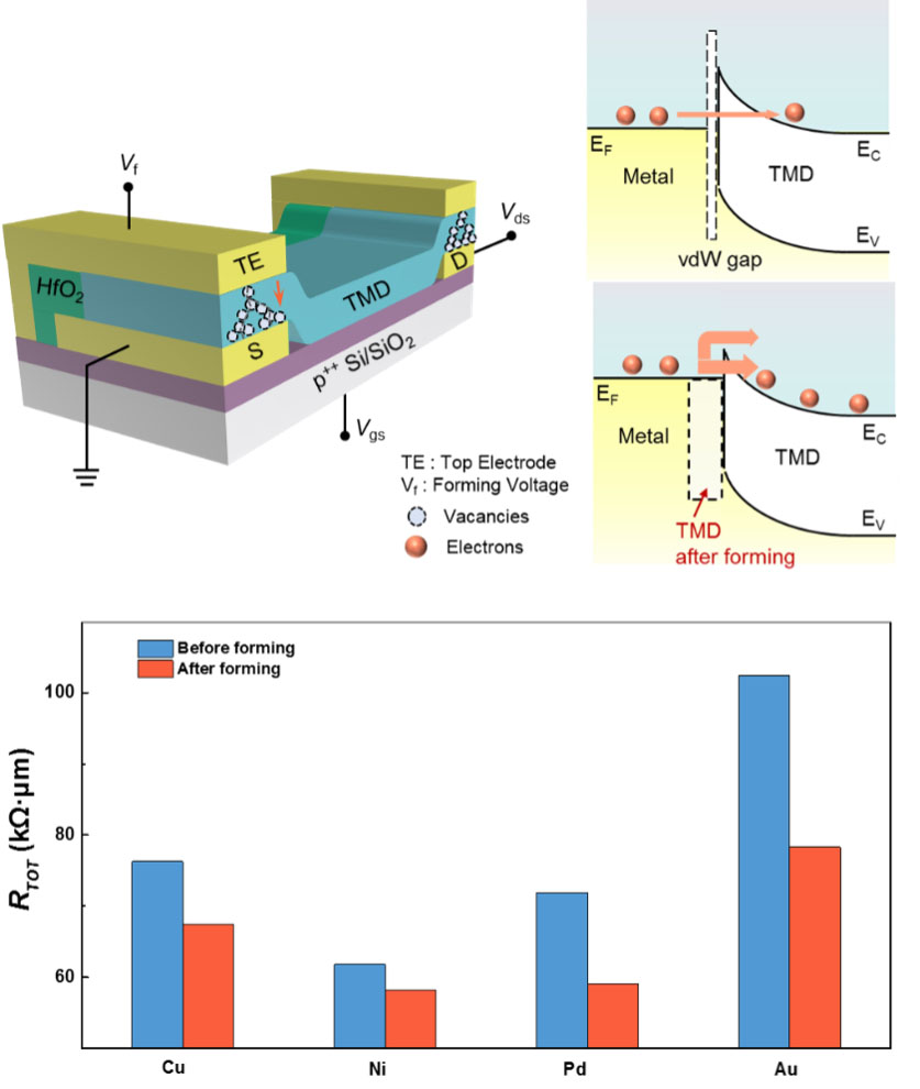
| This is achieved by simply introducing a vertical metal/semiconductor/metal memristor structure at the contact regions. By setting the memristors into a non-volatile low-resistance state through memristive forming, they can reduce the contact resistances of MoS2 field effect transistors (FETs) by at least one order of magnitude, and improve the on-state current densities of MoTe2 FETs by about two orders of magnitude. |
| The researchers also demonstrate that this strategy is applicable to other two-dimensional semiconductors, including MoSe2, WS2 and WSe2, and a variety of contact metals, including Au, Cu, Ni, and Pd. |
| The strategy proposed in their work has good universality on channel and contact metal type, indicating a high technological applicability, which can promote the further developments of 2D semiconductors. |
| Provided by The Hong Kong Polytechnic University |

Become a Spotlight guest author! Join our large and growing group of guest contributors. Have you just published a scientific paper or have other exciting developments to share with the nanotechnology community? Here is how to publish on nanowerk.com. |
