| Oct 26, 2022 |
Physicists realize a tunable photoresponse in twisted bilayer lead iodide homostructure |
| (Nanowerk Spotlight) Near-infrared (NIR) photodetectors play a significant role in many aspects of research and daily life such as in astronomical observation, telecommunications, and medical/chemical sensing. According to Einstein’s photoelectric effect, NIR photodetectors generally rely on narrow band-gap semiconductors (<1.6 eV) such as Si, Ge, InAs, etc. |
| However, the narrow band-gap characteristic makes photodetectors encounter bottlenecks, such as low responsivity and high dark current. The realization of sensitive NIR photodetection by using wide band-gap semiconductors is thus of interest. |
| Recently, twisted-angle-induced unusual electrical and optical properties in van der Waals homostructures have received extraordinary attention although they have rarely been applied to optoelectronic devices. |
| Now, a Chinese research group working on two-dimensional (2D) materials photonics led by Professor Guo Ping Wang and Yupeng Zhang, demonstrated broadband photoresponse capable of overcoming the band-gap limitation of semiconductors in the twisted lead iodide homostructures. |
| The twist angle triggered strong and tunable exciton-phonon coupling leading to the formation of a self-trapped energy level within the band gap, which extends the photoresponse of lead iodide from the ultraviolet to the near-infrared region. |
| The researchers reported their findings in Matter ("Tunable photoresponse in twisted lead iodide homostructures via exciton-phonon coupling"). |
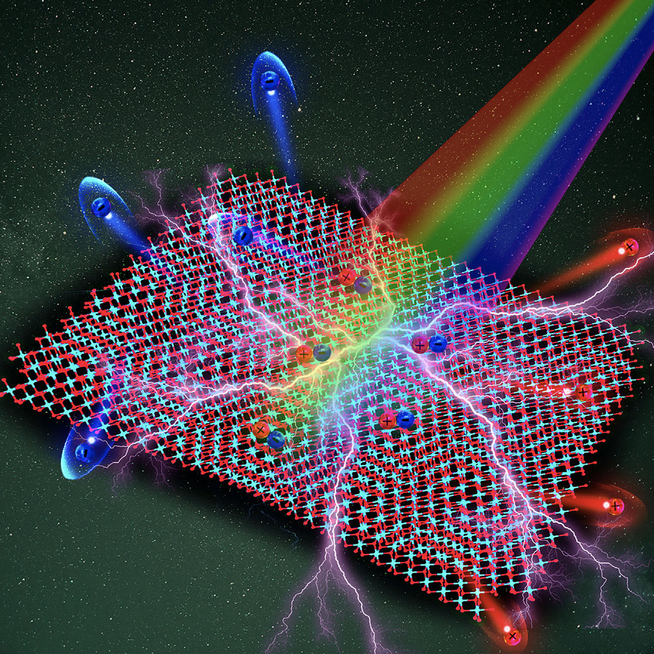 |
| Graphical abstract of this work: Twisted PbI2 homostructures (tPHs) have been successfully synthesized via a simple bottom-up solution epitaxial method. The twist-angle-triggered tunable exciton-phonon coupling in tPHs leads to the formation of a self-trapped energy level within the band gap. As a result, the fabricated photodetectors exhibit a tunable broadband photoresponse. (© CellPress) |
| To realize the practical applications of twistronics – the science of layering and twisting two-dimensional materials to control their electrical properties – it is of the utmost importance to control the interlayer twist angle and interface quality. |
| However, the traditional dry-transfer technique is inappropriate for synthesizing homo- or heterostructures consisting of vertically stacked thick nanoplates (above 10 nm) with an atomically sharp interface. |
| In this work, the researchers developed a bottom-up solution epitaxial method to grow twisted PbI2 homostructures with an atomically sharp interface. By controlling the solution temperature, a transformation from homogeneous to heterogeneous nucleation occurred and induced the formation of twisted PbI2 homostructures. |
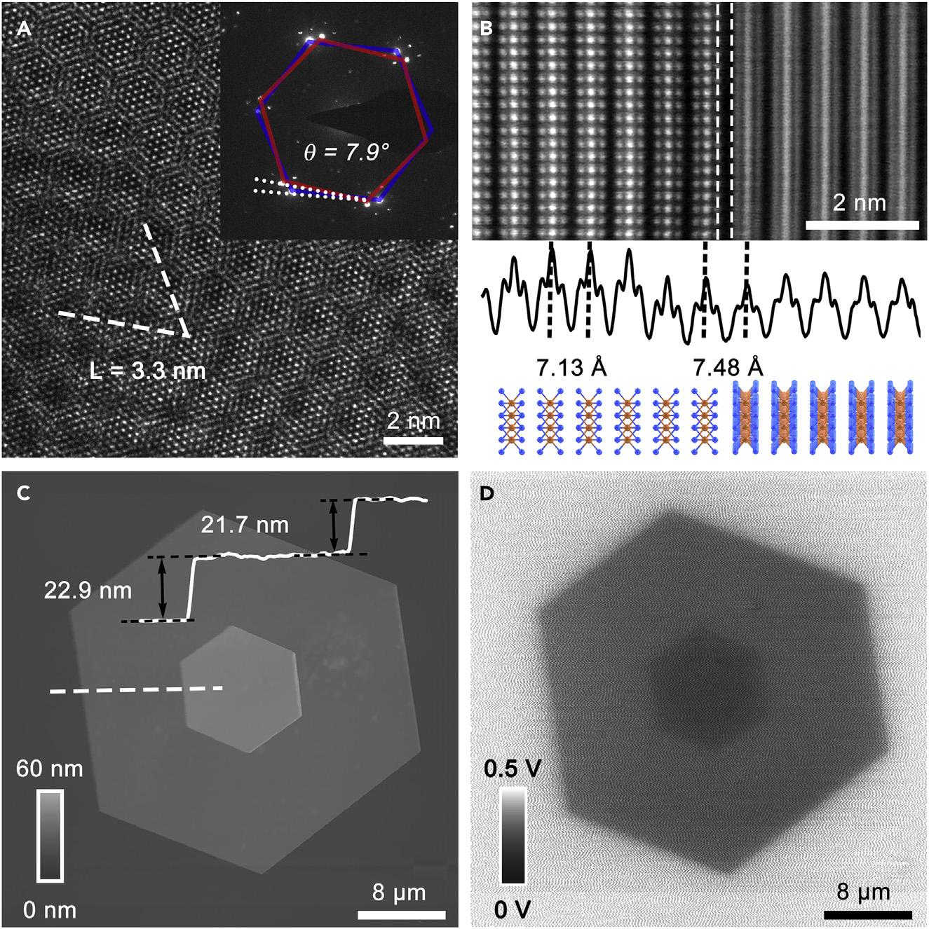 |
| Structural characterization of the twisted PbI2 homostructure. (A) HRTEM image and corresponding SAED pattern taken from the homostructure region of the tPH. (B) Cross-sectional HRTEM image of the vdW interface with the corresponding atomic model and intensity profile (white solid line); the white dashed line indicates the interface of the adjacent nanoplates, and the blue and orange balls represent the I and Pb atoms, respectively. (C) AFM image and corresponding height profile of the q = 2.3° tPH. (D) KPFM image corresponding to the tPH presented in (C). (© CellPress) |
| Both steady-state and temperature-dependent photoluminescence emission spectra indicate that the twisted PbI2 homostructures with different twist angles exhibit strong EPC strength and that the exciton-phonon coupling strength was related to the twist angles. |
| The Huang-Rhys factor can be dramatically enhanced from 0.39 to 20.59. As a result, the formation of a self-trapped energy level within the band gap extends the photoresponse of PbI2 from the ultraviolet to the near-infrared region. |
| The fabricated photodetectors based on twisted lead iodide homostructures exhibit an ultra low dark current (fA level) and a fast response (ms level) as well as a high responsivity from the ultraviolet to near-infrared range (398 mA/W@405 nm and 0.511 mA/W@785 nm). |
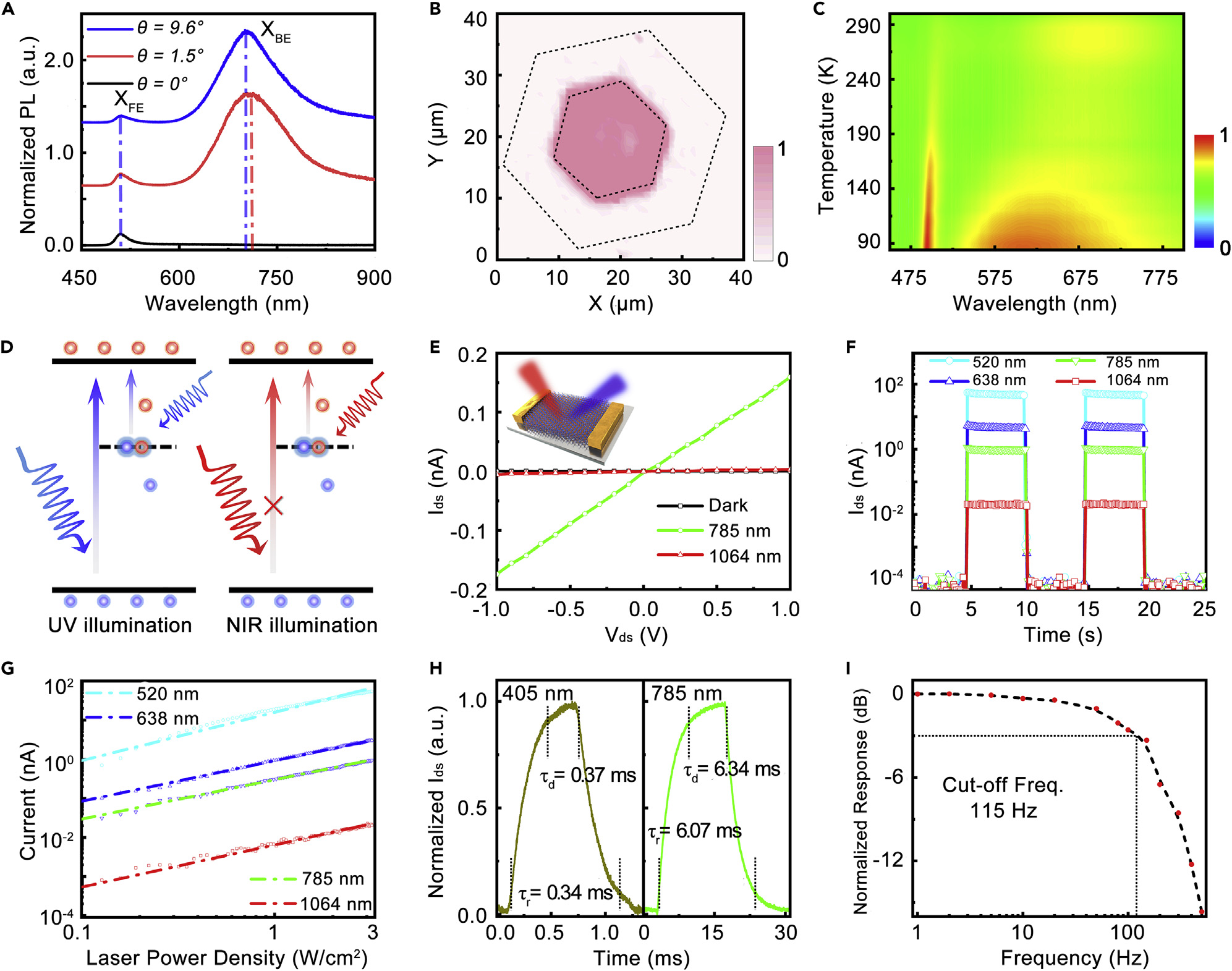 |
| Exciton-phonon coupling and photodetection of the tPHs. (A) PL emission spectra of the tPHs with different twist angles at 300 K. (B) Spatial map of the PL intensity of the XBE of the q = 1.2° tPHs at 300 K. (C) Temperature-dependent PL emission spectra of the tPHs. (D) Schematic illustration of the photogenerated carrier transport under UV- and NIR-light illumination. The blue and red balls represent electrons and holes, respectively. (E) Ids-Vds curves of the tPHs photodetector in dark and under NIR laser illumination (power density = 3.1 W/cm-2); inset: schematic illustration of the tPHs photodetector. (F) Time-resolved on-off curves of the tPHs photodetector under laser illumination at a bias of 5 V (power density = 3 W/cm-2). (G) Power-dependent photocurrents of tPHs photodetector under laser illumination at a bias of 5 V. (H) Temporal response of the tPHs photodetector under 405 and 785 nm laser illumination at a bias of 5 V. (I) Normalized response as a function of the modulation frequency. (© CellPress) |
| This work presents a simple strategy to realize broadband photodetectors and demonstrates the potential of twisted 2D structures for next-generation optoelectronic applications. |
| Provided by College of Electronics and Information Engineering, Shenzhen University, as a Nanowerk exclusive. |

Become a Spotlight guest author! Join our large and growing group of guest contributors. Have you just published a scientific paper or have other exciting developments to share with the nanotechnology community? Here is how to publish on nanowerk.com. |
