| Apr 21, 2023 |
Van der Waals integration permits advanced photonic applications from 2D materials to 3D crystals |
| (Nanowerk Spotlight) Van der Waals (vdW) integration refers to a physical assembly strategy that was originally applied in the two-dimensional (2D) materials and nanotechnology community to construct vdW heterostructures and electronic devices. This method circumvents the fundamental limit of lattice matching and process-compatibility in heteroepitaxy by leveraging film transfer, without necessitating expensive instruments or lengthy development process. It also features unprecedented degrees of freedom in constructing artificial layered vdW structures regardless of the 2D material compositions or crystal parameters. |
| Recent years, however, have witnessed exciting progress on applying vdW integration to photonic and optoelectronic applications, from not only 2D materials but also exfoliated freestanding 3D nanomembranes (Fig. 1). |
| Recent advents on 2D-materials-assited epitaxy and layer lift-off technique have enabled a vast collection of functional single-crystalline three-dimensional (3D) thin films that can also be exfoliated from parent substrate into freestanding thin-films like 2D materials, with artificially defined vdW interfaces for photonic vdW integration. |
| Nanomembranes with diverse optical functionalities, such as electro-optical thin-film lithium niobate, group III-V optical gain media like GaAs, and piezoelectric films AlN, can be readily transferred to arbitrary prefabricated photonic structures such as optical waveguides, micro-resonators, and metasurface for massive novel photonic applications. |
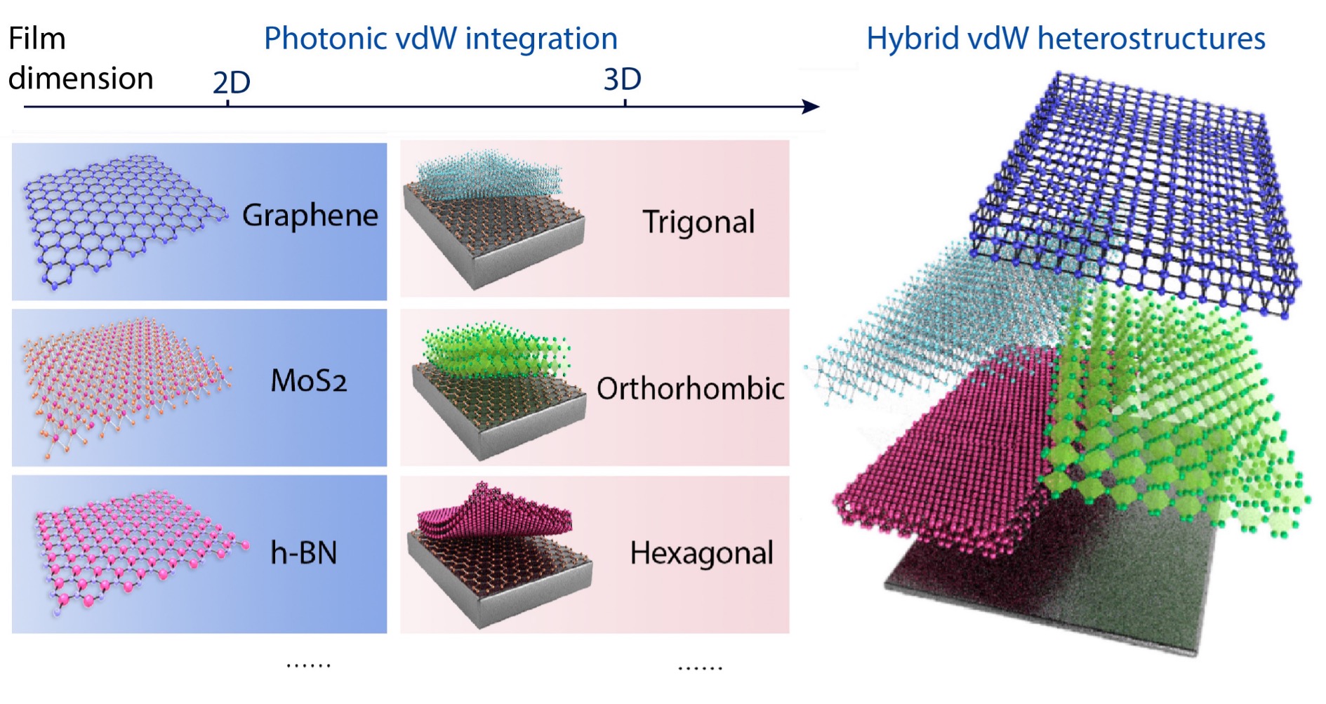 |
| Figure 1. Freestanding 2D and 3D nanomembranes for photonic van der Waals integration. (Image courtesy of the researchers) |
| In a recent paper published on Nature Reviews Materials ("Photonic van der Waals integration from 2D materials to 3D nanomembranes"), a team of international researchers from USA, Singapore, and South Korea have presented a comprehensive review article outlining recent advances on photonic vdW integration. |
| Currently available 2D and 3D vdW building blocks are comprehensively cataloged, with detailed discussions from thin-film preparation to device implementation. Practical challenges that prevent this field migrate into fully fledged technology are elaborated, encompassing scalable nanomembrane production and high-quality layer transfer. Awaiting opportunities are highlighted as well for advanced hetero-integrated photonics, vdW meta-photonics, nanophotonic polaritons, and flexible and bio-compatible optoelectronic applications. |
| Besides, the exfoliation of these single-crystalline nanomembranes also permits the re-use of the costly substrates to largely reduce the cost for non-silicon materials such as GaAs, GaN, InP to foster their further commercialization for photonic integrated circuits and nano-electronics. |
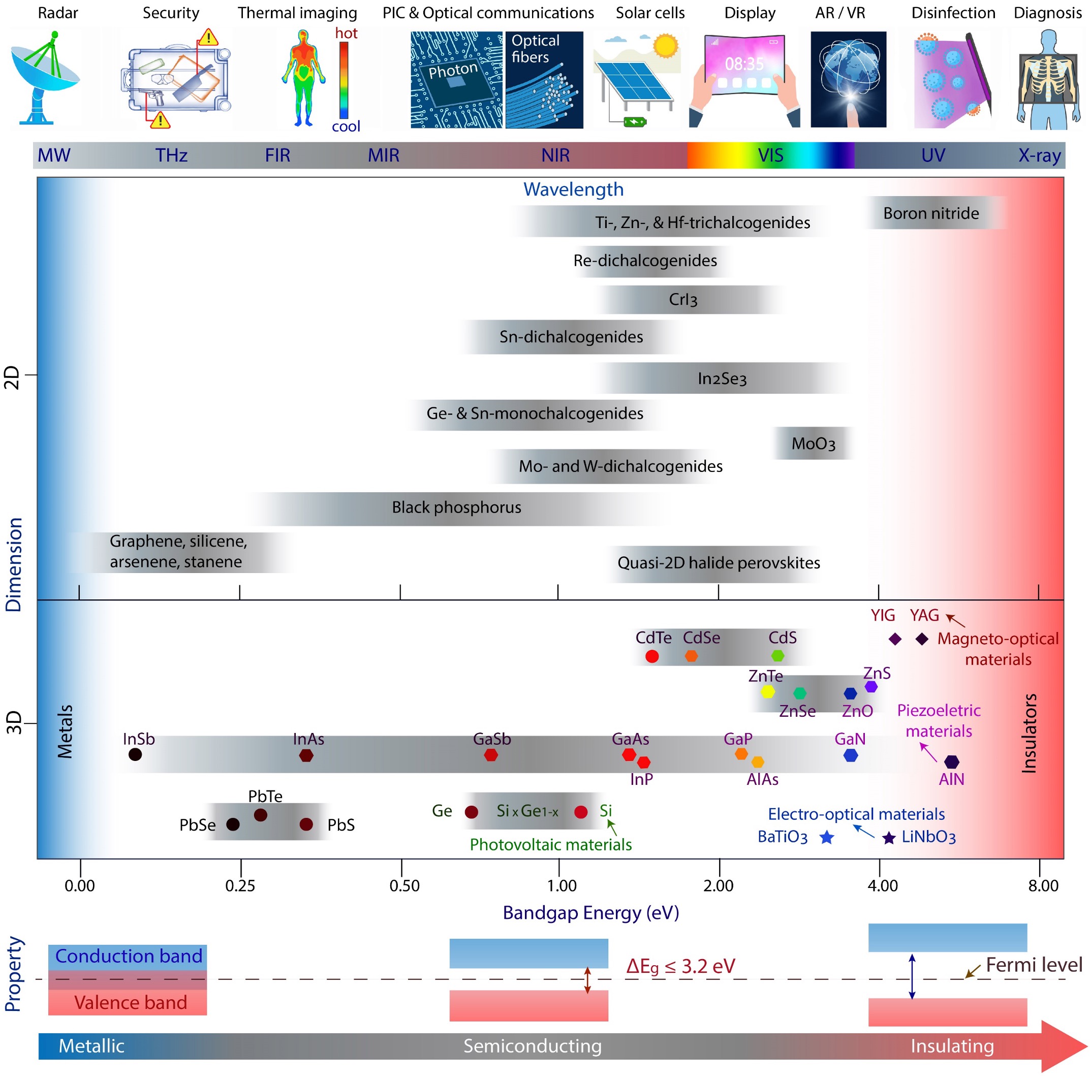 |
| Figure 2. Fundamental attributes of photonic van der Waals films. (Image courtesy of the researchers) |
| As the photonic vdW integration approach can enable previously inaccessible device layouts and hybrid heterostructures by playing around the 2D and 3D vdW thin-film building blocks, the authors envision record-setting novel hetero-integrated photonic devices and exotic nanophotonic physics hatching from mixed-dimensional vdW interfaces. |
| Provided by the University of Washington in St. Louis |

Become a Spotlight guest author! Join our large and growing group of guest contributors. Have you just published a scientific paper or have other exciting developments to share with the nanotechnology community? Here is how to publish on nanowerk.com. |
