| Sep 12, 2023 |
Researchers pioneer atomic-scale patterning and switching in 2D crystals for advanced computing |
| (Nanowerk Spotlight) With atomic-scale thickness, the physical and electronic properties of 2D materials can be easily altered by imposing artificially designed defects, surface modification, or spatially periodic potentials, thus providing an effective way to engineer the functionality of a device as desired. |
| Different from the general defect engineering that is uncontrollable and randomly distributed, patterned structure design, such as moiré superlattice patterns and spatially periodic dielectric structures, can be more precise in manipulating the local atomic and electronic environment on a large scale, thus ensuring the microscopic homogeneity of materials and devices. |
| Yin and colleagues, the researchers from Wuhan University, reported that controllable atomic-scale patterning and resistive switching can be realized in 2D superionic cuprous telluride with rigid Te network and mobile Cu ions, and reached a unique correlation of geometric pattern and device. |
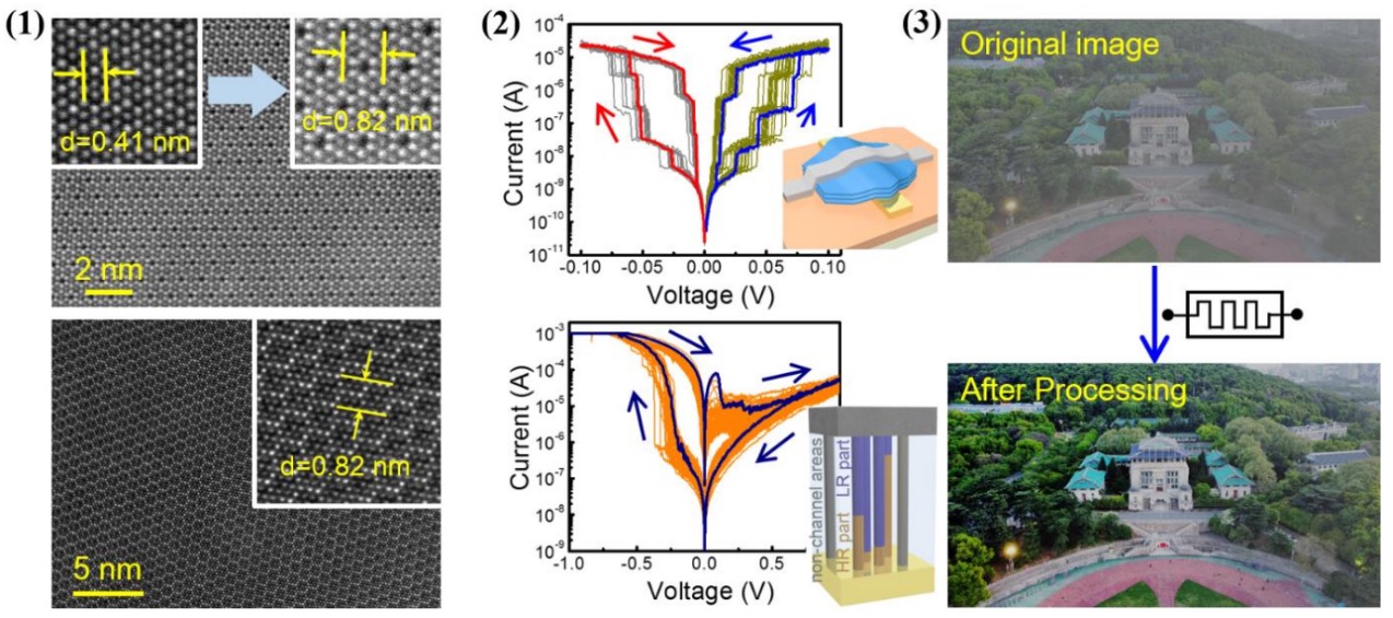 |
| Sample characterizations (single-atom scale patterning), electrical properties (controllable resistive switching), and application in image processing. (Image courtesy of the researchers) |
| The atomic-scale patterning in superionic cuprous telluride is activated by exploiting the bonding difference of Cu atoms at nonequivalent sites. The growth time plays a pivotal role in the formation and distribution of monatomic pores in cuprous telluride crystal. |
| With the designed crystal structure and electrical contact, piezoelectricity-like multi-level switching and nonvolatile bipolar switching, which are triggered by the hopping of Cu ions under electric fields and the formation/disruption of conductive filaments, were achieved respectively. |
| Moreover, a compact model for memristor based on the equivalent resistor topology is developed for mimicking the formation and disruption of conductive filament. Their application in image processing was also demonstrated, by which good dehaze effect was obtained. |
| With high scalability and three-dimensional integration potential, these findings are expected to enable a viable 2D memristor solution for image-processing-related tasks beyond von Neumann computing. |
| This work has been published in the journal Advanced Materials ("Engineering atomic-scale patterning and resistive switching in two-dimensional crystals and application in image processing"). |
| Provided by Wuhan University as a Nanowerk exclusive |

Become a Spotlight guest author! Join our large and growing group of guest contributors. Have you just published a scientific paper or have other exciting developments to share with the nanotechnology community? Here is how to publish on nanowerk.com. |
