| Posted: Oct 09, 2008 |
Changed behavior of collapsed nanotubes has major ramification for nanoelectronics |
| (Nanowerk Spotlight) In contrast to the often depicted model of a perfect hexagonal lattice cylinder shape of carbon nanotubes (CNTs), these nanomaterials often become twisted, bent or otherwise deformed during their growth, processing, or characterization. Researchers have found that some of these defects can be associated with a rearrangement of atoms and bonds which in turn will impact on the band structure and therefore affects the electronic properties of the tube. |
| Previous experimental Atomic Force Microscopy (AFM) and Transmission Electron Microscopy (TEM) studies of carbon nanotubes have clearly identified their susceptibility to collapse and theoretical predictions of the impact that these deformations have on the electronic properties have been formulated. Theoretical calculations of electronic structure postulated that the electronic properties of these systems may be altered when bringing the two opposing layers into close proximity by squashing the tube, and a band gap can be opened or closed in response to the structural perturbation, depending on the nanotube helicity. |
| Experiments at the University of Surrey in the UK are the first to show atomically resolved radially collapsed double-walled carbon nanotubes, bringing also clear evidence of changes in the fundamental electronic behavior of these systems in response to the deformation. |
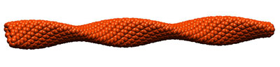 |
| Schematics of a collapsed and twisted carbon nanotube. (Image: Dr. Giusca, University of Surrey) |
| These findings follow on our earlier scanning tunneling microscopy results on collapsed single-walled carbon nanotubes which also confirmed earlier theoretical predictions revealing that the metallic character is maintained provided the squashing does not bring the two flat opposing faces too close to one another ("Atomic and electronic structure in collapsed carbon nanotubes evidenced by scanning tunneling microscopy"). Compared to the single-walled case, for collapsed double-walled nanotubes, comprising of two constituent tubes, one inside another, our results highlight the importance of the interlayer interaction for the collapse and twist deformation, as well as for the electronic behavior of these systems. |
| As reported by our team – including Dr. Ravi P. Silva who heads ATI and Dr. Yann Tison from the Technical University of Denmark – in the September 11, 2008 online edition of Nano Letters ("Evidence for Metal-Semiconductor Transitions in Twisted and Collapsed Double-Walled Carbon Nanotubes by Scanning Tunneling Microscopy"), these findings present strong evidence in support of changes in the fundamental electronic properties in direct relation with the atomic structure when carbon nanotubes are subject to radial deformations and torsional strain. |
 |
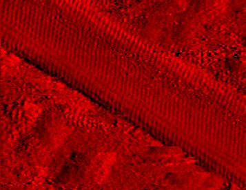
| STM image of a collapsed and twisted double-walled CNT. (Image: Dr. Giusca, University of Surrey) |
| Using a scanning tunneling microscope (STM) – which has the powerful ability of simultaneously resolving the atomic structure, as well as providing information about the electronic structure of materials – reveals that the metallic behavior changes to semiconducting behavior when squashing and twisting carbon nanotubes. |
| Tthe theoretically-predicted relationship between the structure and electronic properties of carbon nanotubes has been confirmed earlier using STM and showed that depending on the nanotube's diameter and on the degree of helicity in the nanotube wrapping, different configurations can result in the tubes behaving either as a metallic conductor or as a semiconductor. |
| The relationship between the structure and the electronic behavior is valid for nanotubes displaying the perfect honeycomb carbon lattice, without any structural or topological defects. However, the situation is different in practice and nanotubes have been found to develop various defects during their synthesis and processing, which are all known to affect their electronic behavior. |
| In addition to bending and twisting, the two most known types of structural deformations, nanotubes can also display the collapsed state configuration, when the nanotubes appear squashed. This particular type of deformation was theoretically explained to occur when the interlayer interaction between opposing sides of the nanotube balances the energy due to the nanotube curvature. |
| These results pass on a cautionary note in the design of semiconductor components based on carbon nanotubes and for their future integration with conventional existing electronic technologies, where, for example fabrication methods can induce deformations by placing control electrodes on top of nanotubes or by embedding the nanotubes into other structures. Chief among these structures would be the use of carbon nanotubes as interconnects for the billion dollar semiconductor industry, for which the deformation and mechanical integrity of these components should be of paramount importance. |
 |
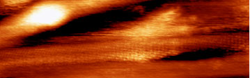
| STM image of a collapsed SWNT. (Image: Dr. Giusca, University of Surrey) |
| The findings also present relevance for matters concerning the characterization of these structures, as most of the electronic transport measurements are performed using various metals to contact the nanotubes and the measured values could in this case be affected by hidden contributions. |
| Apart from providing a remarkable confirmation of theoretical expectations, our findings are of significant importance for nanoscale applications, pointing to the possibility of a reversible metal-semiconductor junction created by squashing and twisting the nanotubes. |
| High conformational deformations – similar to the ones we present in the Nano Letters paper – have been shown by computer simulations to significantly enhance locally the chemical reactivity of carbon nanotubes, meaning that controlled deformations could also find prospective applications for potential sensing devices. |
| This work should pose an excellent challenge to experimentalists to create ingenious ways which allow deforming carbon nanotubes in a controllable manner to simply provide the metallic or semiconducting features required by specific applications. The most significant direction will of course be in the area of interconnects for semiconductor chips. We will be working closely with colleagues in academia and industry to understand the fundamentals of using this unique material, carbon nanotubes, for satisfying the needs of high current conduction with little or no electromigration of the constituent material. |
| By Dr. Cristina E. Giusca, Research Fellow, Advanced Technology Institute, School of Electronics and Physical Sciences, University of Surrey. Copyright Nanowerk LLC |

Become a Spotlight guest author! Join our large and growing group of guest contributors. Have you just published a scientific paper or have other exciting developments to share with the nanotechnology community? Here is how to publish on nanowerk.com. |
