Paintable 'second skin' gel for wearable bioelectronic sensors
 Researchers have developed an on-skin paintable waterproof biohydrogel for wearable bioelectronics, enabling high-fidelity monitoring of bioelectrical signals like ECG.
 Subscribe to our Nanotechnology Spotlight feed
Researchers have developed an on-skin paintable waterproof biohydrogel for wearable bioelectronics, enabling high-fidelity monitoring of bioelectrical signals like ECG.
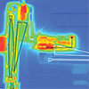 Researchers have developed innovative mechanical transistors that combine temperature-responsive materials and switchable structures, enabling complex logic operations and memory storage without electricity, opening up new possibilities for computing and environmental interaction.
 Researchers demonstrate highly deformable micro-supercapacitors using laser-patterned liquid metal electrodes, addressing key challenges in flexible energy storage.
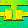 Exploring gate metal work function impact on nanoscale transistor performance for advanced electronics innovation and efficiency.
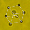 Researchers have developed a method for precisely controlling the 3D arrangement of microscopic particles using laser light and a phase-changing gel medium.
 Revolutionary bioresorbable films extend life of implantable electronics, dissolving safely after use.
 Novel spiking neural network architecture processes images using event-driven photodetector circuits inspired by biological vision. Direct optical-to-spike conversion slashes power needs for visual pattern recognition tasks.
 Researchers develop 100-nanometer-thick 'aramid nanodielectric' films ideal for skin-mounted electronics like sweat-immune medical sensors and flexible computer circuits thinner than human hair.