| Mar 17, 2024 |
Optimizing nanoscale transistor performance through gate metal work function selection |
| (Nanowerk Spotlight) For new generation electronic appliances advanced nanoscale transistors are in demand which needs precise biasing of each device. These stringent biasing conditions can be relaxed by obtaining precise values of the threshold voltages of the transistor. This will also improve tolerance of digital logic states to electrical noise. The requirements of reduced power consumption are achieved in CMOS field-effect transistors (FETs) by fabricating and operating it in enhancement (E) mode i.e. absence of free charge carriers in the channel at zero gate voltage. |
| To clarify, in the context of field-effect transistors, enhancement mode (E-mode) refers to the state where the device requires a certain gate voltage to induce a conducting channel between the source and drain terminals. Conversely, depletion mode (D-mode) FETs inherently have a conducting channel at zero gate voltage, requiring a gate voltage of opposite polarity to 'deplete' or turn off the channel. This fundamental distinction plays a crucial role in how devices are designed for specific applications, impacting their power consumption, speed, and overall functionality. |
| On the other hand, depletion (D) mode transistors have higher currents than enhancement mode due to ample charge carrier density. In contrast to switching application of FET, for high-frequency applications off-state of FET is not a compulsory requirement. In fact, the presence of a channel at zero gate bias is advantageous to obtain high transconductance at lower voltages. For Si FETs, the enhancement or depletion modes were determined at the fabrication step of ion implantation doping. However, it is challenging to implement this solution for the new generation of thin materials like organic semiconductors and 2D materials. |
| According to new research published in the journal of ACS Applied Electronic Materials ("Selective Operation of Enhancement and Depletion Modes of Nanoscale Field-Effect Transistors"), by choosing a particular work function for a gate metal, threshold voltages of the p-type FETs can be changed from negative to positive values that is selective switching between enhancement mode to depletion mode of the operation. |
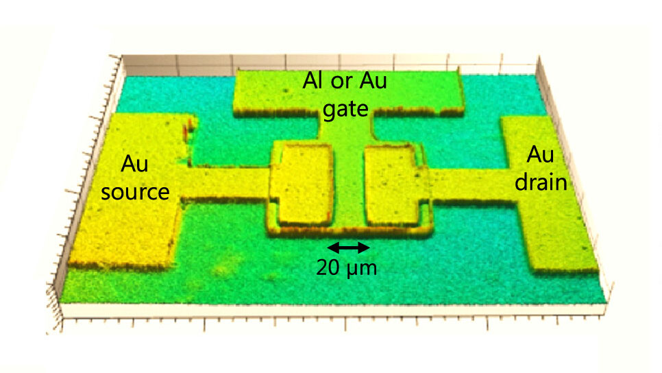 |
| 3D optical profiler image of the fabricated FETs. (Reprinted with permission by American Chemical Society) |
| The researchers experimentally fabricated the FETs with various gate metal electrodes having different work functions. The dielectric alumina thickness was just 5 nm. Due to this short separation between gate metal and organic p-type semiconducting channel, there is electrostatic interaction between them even without the application of external voltage. When low-work function metal like aluminum (4.4 eV) is used, the FET operates in E-mode. For high-work function gate metals like gold (5.0 eV), a certain number of holes are induced in the channel at zero gate voltage. This leads to a good amount of current in the channel which is known as D-mode operation. |
| Complementing their groundbreaking experimental efforts, the research team employed advanced TCAD device simulations, which were instrumental in validating their findings. These simulations, producing color contour plots of induced hole density, provided both a visual and theoretical verification of the influence of gate metal work functions on the FETs' operational modes. This comprehensive approach, marrying experimental data with simulation insights, not only enhances the credibility of the research but also emphasizes its significance for technological advancements and potential for scale-up in manufacturing. |
| The lead author Dr Abhay Sagade from SRMIST, India, revealed that the observed effects are profound for thin dielectric thickness such as less than 10 nm. "For the larger thicknesses, the FETs remain in enhancement mode even for high work function gate metals," he notes. "This concept can be easily extendable to any thin organic, inorganic and new generation 2D materials." |
| An important aspect of this study is the focus on the thickness of the dielectric layer used in FETs. Researchers found that the effects observed—switching between enhancement and depletion modes—were pronounced for thin dielectrics, specifically those less than 10 nm. This finding highlights the critical role of dielectric thickness in influencing FET behavior, emphasizing the need for precise control over material properties to achieve desired device performance. |
| Using this method, it should be possible to fabricate more compact-sized accurate and reconfigurable digital logic, and oscillator devices and circuits. Further, D-mode OFETs with improved currents can be utilized efficiently for high-frequency applications. This also has immense implications for upcoming quantum devices and technological applications which use small dimensional sensitive devices. |
| Beyond the immediate benefits for digital logic and oscillator devices, the ability to selectively switch between operation modes holds immense promise for high-frequency applications, potentially revolutionizing the design of next-generation quantum devices. The versatility of this method paves the way for innovative electronic components that are not only more efficient and compact but also highly reconfigurable, meeting the diverse needs of modern technology landscapes. |
 By
Michael
Berger
– Michael is author of four books by the Royal Society of Chemistry:
Nano-Society: Pushing the Boundaries of Technology (2009),
Nanotechnology: The Future is Tiny (2016),
Nanoengineering: The Skills and Tools Making Technology Invisible (2019), and
Waste not! How Nanotechnologies Can Increase Efficiencies Throughout Society (2025)
Copyright ©
Nanowerk LLC
By
Michael
Berger
– Michael is author of four books by the Royal Society of Chemistry:
Nano-Society: Pushing the Boundaries of Technology (2009),
Nanotechnology: The Future is Tiny (2016),
Nanoengineering: The Skills and Tools Making Technology Invisible (2019), and
Waste not! How Nanotechnologies Can Increase Efficiencies Throughout Society (2025)
Copyright ©
Nanowerk LLC
|

Become a Spotlight guest author! Join our large and growing group of guest contributors. Have you just published a scientific paper or have other exciting developments to share with the nanotechnology community? Here is how to publish on nanowerk.com. |
