

Nanotechnology News – Latest Headlines
Fraunhofer Center Nanoelectronic Technologies and Tokyo Electron intensify cooperation
The institute acquired an automatic TEL wafer prober in order to meet the requirements of latest measuring tasks related to capacity, quality and positioning accuracy within a large temperature range. Moreover future wafer test and characterization requirements will be developed and verified by means of an additional system.
November 3, 2011 Read more
EU nanoelectronics project investigates new components for future computer memories
An EU-funded project investigates 11-nm FinFET variability and its impact on embedded memories.
November 3, 2011 Read more

EU project IMOLA starts R+D on large-area, intelligent OLED lighting
Imec and its project partners announce the launch of IMOLA (Intelligent light Management for OLED on foil Applications), a project under the EU's 7th framework program for ICT (FP7).
November 3, 2011 Read more
Physicists identify room temperature quantum bits in widely used semiconductor
A discovery by physicists at UC Santa Barbara may earn silicon carbide - a semiconductor commonly used by the electronics industry - a role at the center of a new generation of information technologies designed to exploit quantum physics for tasks such as ultrafast computing and nanoscale sensing.
November 2, 2011 Read more
UCLA Engineering researchers awarded $4.5M to develop stronger carbon nanotube materials
Researchers at the UCLA Henry Samueli School of Engineering and Applied Science have been awarded $4.5 million over four years by the U.S. Department of Defense to strengthen carbon nanotube yarns and sheets, materials that hold great promise for advancing satellite technology.
November 2, 2011 Read more
Printing Technologies for conventional electronics: A step closer to fully printed devices
During IDTechEx's Printed Electronics and Photovoltaics USA conference and tradeshow in Santa Clara this November 30 - December 1, attendees will have the opportunity to tour the facilities of Applied Materials.
November 2, 2011 Read more
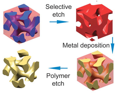
Chemically assembled metamaterials could lead to superlenses and cloaking
Uli Wiesner's research group at Cornell offers a method they have pioneered in other fields, using block copolymers to self-assemble 3-D structures with nanoscale features.
November 2, 2011 Read more
Manufacturing microscale medical devices for faster tissue engineering
New laser technique could be used for production of tissue scaffolds, microneedles.
November 2, 2011 Read more
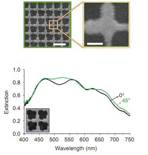
Solar power could get boost from new light absorption design
Solar power may be on the rise, but solar cells are only as efficient as the amount of sunlight they collect. Under the direction of a new McCormick professor, researchers have developed a new material that absorbs a wide range of wavelengths and could lead to more efficient and less expensive solar technology.
November 2, 2011 Read more
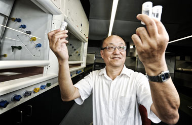
Nanotechnology makes storing radioactive waste safer
Queensland University of Technology researchers have developed new technology capable of removing radioactive material from contaminated water and aiding clean-up efforts following nuclear disasters.
November 2, 2011 Read more
ERA-Net EuroNanoMed allocates 8 million euros to European research projects in nanomedicine
Eight projects from 11 countries were chosen to be funded as part of the 3rd and last call.
November 2, 2011 Read more
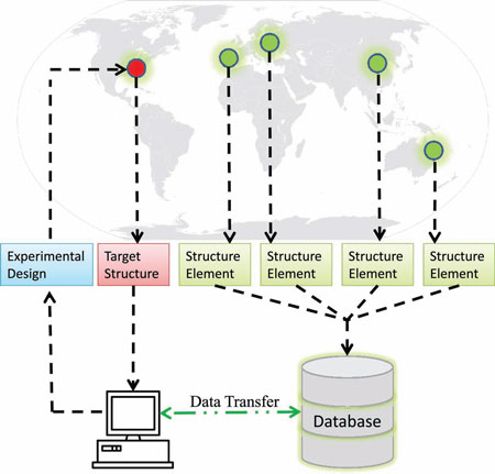
Initiation of a database of functional micro- and nanostructures
Writing in a recent issue of Small, Professor Ned Thomas, Dean of Engineering at Rice University, proposes the setup of a database of functional nanostructures.
November 2, 2011 Read more
Graphene applications in electronics and photonics
Phaedon Avouris, manager of the Nanometer Scale Science and Technology division at IBM's T.J. Watson Research Center in Yorktown Heights, N.Y., will present new experimental results on the use of graphene in fast electronics and photonics at the AVS meeting in Nashville, Tenn., held Oct. 30 - Nov. 4.
November 2, 2011 Read more

Exploring the inner workings of materials
From concrete to cancer cells, Van Vliet brings an engineer's mindset to the study of biology and materials.
November 2, 2011 Read more

Nanotechnology Christmas gift: A $8000 tie with gold nanocoating
A nanometer-thin layer of pure gold now lends ties and pocket handkerchiefs that authentic gold sheen, thanks to a new Empa-developed process.
November 1, 2011 Read more
World leading centre of excellence in vibrometry to be established at University of Leicester
The University of Leicester has been allocated GBP1.07 million towards a GBP5.6 million hi-tech project supporting and impacting advanced engineering and manufacturing automotive, aerospace and space industry sectors.
November 1, 2011 Read more
 Subscribe to our Nanotechnology News feed