Electron Holography: Unveiling the Nanoscale World
What is Electron Holography?
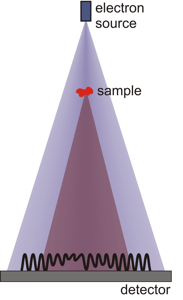
Electron holography is an advanced microscopy technique that utilizes the wave nature of electrons to record and reconstruct the complete information about an object, including both amplitude and phase. By capturing the interference pattern formed by the interaction of an electron beam with a specimen, electron holography enables the visualization and quantitative analysis of nanoscale structures, electric and magnetic fields, and material properties with unprecedented resolution and sensitivity.
Principles of Electron Holography
Electron holography is based on the fundamental principles of holography, which involves the recording and reconstruction of wavefronts. In holography, a hologram is created by capturing the interference pattern formed when a coherent light source, such as a laser, illuminates both the object of interest and a reference beam. This interference pattern contains both amplitude and phase information about the object. When the hologram is illuminated with the reference beam, the original wavefront is reconstructed, creating a three-dimensional image of the object that exhibits depth and parallax. In electron holography, the same principles are applied, but instead of using light, coherent electron beams are employed to record and reconstruct the wavefronts, enabling the visualization and analysis of nanoscale structures and phenomena.
The key concepts underlying electron holography include:
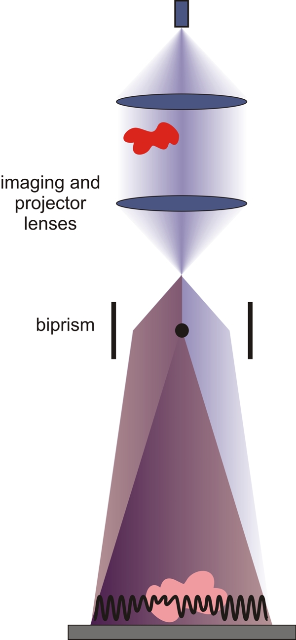
- Interference: In electron holography, an electron beam is split into two parts: the object wave, which interacts with the specimen, and the reference wave, which passes through vacuum. These two waves are then brought together to form an interference pattern, known as a hologram.
- Phase Information: The phase of the electron wave is sensitive to the electrostatic potential and magnetic vector potential of the specimen. By measuring the phase shift induced by the specimen, electron holography can provide quantitative information about the local electric and magnetic fields, as well as the specimen's thickness and mean inner potential.
- Reconstruction: The recorded hologram contains both amplitude and phase information. By applying a reconstruction process, which involves illuminating the hologram with a reference wave, the original object wave can be reconstructed, revealing the complete information about the specimen.
Types of Electron Holography
There are two main types of electron holography, each with its own advantages and applications:
Off-Axis Electron Holography
Off-axis electron holography is the most commonly used technique, where the object wave and reference wave are spatially separated in the hologram. This is achieved by using an electrostatic biprism, which acts as a beam splitter and recombiner. Off-axis electron holography provides a direct and quantitative measurement of the phase shift induced by the specimen, enabling the mapping of electric and magnetic fields with high sensitivity.
In-Line Electron Holography
In-line electron holography, also known as Gabor holography, uses a single electron beam that passes through both the specimen and vacuum. The interference between the scattered and unscattered waves forms an in-line hologram. While in-line electron holography has a simpler setup compared to off-axis holography, it requires more complex reconstruction algorithms to separate the twin images and retrieve the phase information.
Applications of Electron Holography
Electron holography has found numerous applications in the characterization of nanoscale materials and devices, including:
- Electric and Magnetic Field Mapping: Electron holography can directly visualize and quantify the electric and magnetic fields in and around nanostructures, such as quantum dots, nanowires, and thin films. This capability is crucial for understanding the electronic and magnetic properties of nanomaterials and designing novel devices.
- Dopant Profiling: By measuring the phase shift induced by the mean inner potential, electron holography can map the dopant distribution in semiconductor devices with nanometer resolution. This information is essential for optimizing device performance and reliability.
- Strain Analysis: Electron holography can reveal the strain fields in crystalline materials by measuring the phase gradient. This technique is particularly useful for studying the strain distribution in nanocomposites, heterostructures, and devices under mechanical or thermal stress.
- Biological Imaging: Electron holography has been applied to image biological specimens, such as proteins and viruses, with high contrast and resolution. By exploiting the phase contrast mechanism, electron holography can visualize low-atomic-number materials that are challenging to image with conventional electron microscopy techniques.
Challenges and Future Perspectives
Despite its powerful capabilities, electron holography faces several challenges that limit its widespread adoption. One of the main challenges is the requirement for highly coherent electron sources, such as field emission guns, which are not readily available in all electron microscopes. Additionally, the reconstruction process in electron holography is computationally intensive and requires specialized software and expertise.
Future developments in electron holography will focus on improving the spatial and temporal resolution, as well as the sensitivity to electric and magnetic fields. The integration of aberration correctors and monochromators in electron microscopes will enable the acquisition of high-quality holograms with sub-nanometer resolution. Furthermore, the development of advanced reconstruction algorithms and machine learning techniques will accelerate the processing and interpretation of electron holography data, opening up new possibilities for the characterization of complex nanoscale systems.
Further Reading
Reports on Progress in Physics, Electron holography—basics and applications
