Transmission Electron Microscopy (TEM)
Definition: Transmission Electron Microscopy (TEM) is a microscopy technique that uses a beam of electrons to visualize specimens at the atomic or molecular level, offering unparalleled resolution and depth of information.
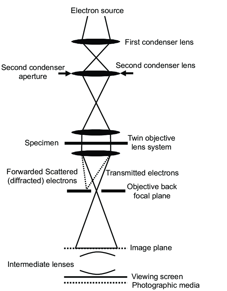
Principle of Operation
TEM works by transmitting a beam of electrons through an ultra-thin specimen. As the electrons interact with the specimen, they are scattered or transmitted, producing an image that is magnified and focused onto an imaging device, such as a fluorescent screen, photographic plate, or sensor. The varying degrees of electron scattering or absorption by different components of the specimen result in variations in contrast in the image, allowing for the observation of structures down to the atomic scale.
Key Features of TEM
- High Resolution: TEM is capable of imaging at a resolution high enough to see individual atoms, making it one of the most powerful tools for materials science, biology, and nanotechnology.
- Structural Analysis: It can provide detailed information about the structure, crystallography, and morphology of materials.
- Chemical Composition: Using techniques such as electron energy loss spectroscopy (EELS) within TEM, it is possible to analyze the chemical composition and electronic structure of materials.
- Dynamic Experiments: TEM can be used for in-situ experiments, including observing reactions at the atomic scale in real time under controlled environments.
Limitations
Despite its advantages, TEM also has limitations:
- Sample Preparation: Specimens must be very thin (typically less than 100 nanometers) to allow electrons to pass through, which can be difficult to achieve for certain materials.
- Damage to Sensitive Samples: The high-energy electron beam can damage biological specimens and some materials.
- Vacuum Requirement: TEM requires a vacuum to operate, which can limit the analysis of materials that are volatile or affected by vacuum conditions.
- Complexity and Cost: Operating a TEM and interpreting the results requires specialized training, and the equipment itself is expensive.
Applications
TEM is utilized in a wide range of fields for its detailed imaging capabilities:
- Materials Science: For characterizing the nanostructure of metals, ceramics, polymers, and composites.
- Biology: In the examination of cellular structures, viruses, and proteins at the molecular level.
- Nanotechnology: For the development and analysis of nanomaterials and devices, including the observation of quantum dots, nanowires, and graphene layers.
- Chemistry: To understand the morphology and structure of catalysts and other chemical compounds.
- Photonics and Electronics: Analyzing the structural integrity and interfaces of photonic crystals and semiconductor devices at the nanoscale.
- Energy Storage and Conversion: Investigating the microstructure of batteries and fuel cells to improve their efficiency and lifetime.
Comparing STEM to TEM
Scanning Transmission Electron Microscopy (STEM) and Transmission Electron Microscopy (TEM) are two closely related imaging techniques used in material science, nanotechnology, and biology for obtaining high-resolution images of samples at the atomic or molecular level. Despite their similarities, there are key differences in their operation and the type of information they provide.
Principle of Operation
STEM operates by scanning a focused electron beam across the sample and detecting the electrons that are transmitted through it. This scanning process allows for the collection of various signals generated by electron-sample interactions, such as secondary electrons, backscattered electrons, and X-rays, providing versatile imaging and analytical capabilities.
TEM, on the other hand, illuminates the sample with a broad electron beam and forms an image from the electrons transmitted through the sample. The image is directly projected onto a detector or a photographic plate, enabling the observation of the internal structure of the sample at high resolutions.
Image Formation and Resolution
In STEM, the image is formed pixel by pixel as the beam scans across the sample, allowing for high-resolution imaging and the ability to perform analytical techniques, such as energy-dispersive X-ray spectroscopy (EDX) or electron energy loss spectroscopy (EELS), at specific points of interest.
In TEM, the entire image is formed at once, providing a global view of the sample. TEM typically achieves high-resolution images with greater detail in the structure of the sample. However, it lacks the analytical capabilities of STEM at specific points within the sample.
Applications and Suitability
STEM is particularly suited for analyzing the composition and electronic structure of materials at the nanoscale, thanks to its ability to collect multiple signals and perform localized analysis.
TEM is ideal for studying the morphology, crystal structure, and defects of materials. It is highly valued for its ability to provide detailed images of the internal structure of samples.
Both STEM and TEM are indispensable tools in the field of microscopy, each with its advantages and specific applications. The choice between STEM and TEM depends on the specific requirements of the study, including the type of information needed about the sample, the resolution required, and the analytical capabilities desired.
Further Reading
Mineralogical Magazine, Transmission electron microscopy (TEM) of Earth and planetary materials: A review
