Scanning Transmission Electron Microscopy (STEM) Explained
Definition: Scanning Transmission Electron Microscopy (STEM) is a cutting-edge imaging technique that combines the principles of scanning electron microscopy (SEM) and traditional transmission electron microscopy (TEM) to offer high-resolution images of the internal structure of materials at the atomic or molecular level.
Definition and Principle of Operation
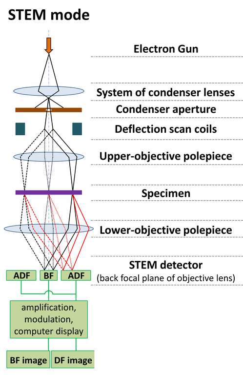
STEM operates by focusing a beam of electrons into a narrow probe that is scanned across a thin specimen. As the electrons interact with the sample, they are either scattered or transmitted. The transmitted electrons are collected by a detector, creating an image that maps the sample's internal structure with exceptional detail.
How STEM Works
The technique involves directing a focused beam of electrons onto a sample and detecting the electrons that are transmitted through it. The intensity of the transmitted electrons at each point creates a high-resolution image that reflects the sample's atomic or molecular structure. STEM is capable of producing images with spatial resolution down to the atomic level, thanks to the fine electron probe it utilizes.
Key Features of STEM
STEM is distinguished by several key features:
- High-Resolution Imaging: STEM's ability to focus electron beams into extremely fine probes allows for imaging at atomic resolutions, making it an essential tool for observing the fine details of material structures.
- Material Composition Analysis: Combined with analytical techniques such as energy-dispersive X-ray spectroscopy (EDX), STEM can identify the elemental composition of materials, providing both structural and chemical information.
- Three-Dimensional Imaging: By tilting the sample and acquiring images from different angles, STEM can be used to reconstruct three-dimensional models of the sample's internal structure.
- Versatility: STEM can be applied to a wide variety of materials, including metals, ceramics, semiconductors, and biological specimens, making it a versatile tool in many fields of research and industry.
Applications of STEM
STEM has a broad range of applications:
- Materials Science: In materials science, STEM is used to study the atomic structure and defects of materials, aiding in the development of new materials with improved properties.
- Nanotechnology: In nanotechnology, STEM is critical for imaging nanoscale structures and devices, facilitating the design and optimization of nanomaterials and nanodevices.
- Electronics: The electronics industry relies on STEM for the characterization of semiconductor devices and materials, helping to improve the performance and reliability of electronic components.
- Life Sciences: STEM also finds applications in the life sciences, providing insights into the structure of cells and viruses at the molecular level.
Comparing STEM to TEM
Scanning Transmission Electron Microscopy (STEM) and Transmission Electron Microscopy (TEM) are two closely related imaging techniques used in material science, nanotechnology, and biology for obtaining high-resolution images of samples at the atomic or molecular level. Despite their similarities, there are key differences in their operation and the type of information they provide.
Principle of Operation
STEM operates by scanning a focused electron beam across the sample and detecting the electrons that are transmitted through it. This scanning process allows for the collection of various signals generated by electron-sample interactions, such as secondary electrons, backscattered electrons, and X-rays, providing versatile imaging and analytical capabilities.
TEM, on the other hand, illuminates the sample with a broad electron beam and forms an image from the electrons transmitted through the sample. The image is directly projected onto a detector or a photographic plate, enabling the observation of the internal structure of the sample at high resolutions.
Image Formation and Resolution
In STEM, the image is formed pixel by pixel as the beam scans across the sample, allowing for high-resolution imaging and the ability to perform analytical techniques, such as energy-dispersive X-ray spectroscopy (EDX) or electron energy loss spectroscopy (EELS), at specific points of interest.
In TEM, the entire image is formed at once, providing a global view of the sample. TEM typically achieves high-resolution images with greater detail in the structure of the sample. However, it lacks the analytical capabilities of STEM at specific points within the sample.
Applications and Suitability
STEM is particularly suited for analyzing the composition and electronic structure of materials at the nanoscale, thanks to its ability to collect multiple signals and perform localized analysis.
TEM is ideal for studying the morphology, crystal structure, and defects of materials. It is highly valued for its ability to provide detailed images of the internal structure of samples.
Both STEM and TEM are indispensable tools in the field of microscopy, each with its advantages and specific applications. The choice between STEM and TEM depends on the specific requirements of the study, including the type of information needed about the sample, the resolution required, and the analytical capabilities desired.
Recent Technological Advancements in STEM
Technological advancements have significantly enhanced STEM's capabilities, including the development of aberration correctors that improve resolution, and the integration of sophisticated detectors that allow for more detailed and comprehensive analysis of materials.
The continuous evolution of STEM technology promises to unlock new possibilities in the characterization and manipulation of materials at the atomic scale, contributing to advances in numerous scientific and industrial fields.
Further Reading
Annual Review of Materials Research, Quantitative Scanning Transmission Electron Microscopy for Materials Science: Imaging, Diffraction, Spectroscopy, and Tomography
Nature Reviews Methods Primers, Machine learning in scanning transmission electron microscopy
Journal of Analytical Science and Technology, Material structure, properties, and dynamics through scanning transmission electron microscopy
