| Posted: Dec 03, 2014 |
New technique simultaneously determines nanomaterials' chemical makeup, topography |
| (Nanowerk News) A team of researchers from the U.S. Department of Energy's Argonne National Laboratory and Ohio University have devised a powerful technique that simultaneously resolves the chemical characterization and topography of nanoscale materials down to the height of a single atom ("Elemental Fingerprinting of Materials with Sensitivity at the Atomic Limit"). |
| The technique combines synchrotron X-rays (SX) and scanning tunneling microscopy (STM). In experiments, the researchers used SX as a probe and a nanofabricated smart tip of a STM as a detector. |
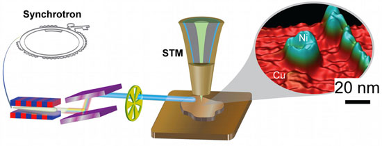 |
| The synchrotron X-ray scanning tunneling microscopy concept allowed Argonne National Laboratory and Ohio University researchers to achieve a recording-breaking resolution of a nanoscale material. They combined of a synchrotron X-ray as a probe and a nanofabricated smart tip as a detector to fingerprint individual nickel clusters on a copper surface at a two-nanometer resolution and at the ultimate single-atomic height sensitivity. And by varying the photon energy, researchers successfully measured photoionization cross sections of a single nickel nanocluster – opening the door to new opportunities for chemical imaging of nanoscale materials. |
| Using this technique, researchers detected the chemical fingerprint of individual nickel clusters on a copper surface at a two-nanometer (nm) lateral resolution, and at the ultimate single atom height sensitivity. By varying the photon energy, the researchers used the difference in photoabsorption cross sections for nickel and the copper substrate to chemically image a single-nickel nanocluster - thus opening the door to new opportunities for chemical imaging of nanoscale materials. Until now, a spatial limit of about only 10-nm was attainable, and the researchers would simultaneously sample a large sample area. The researchers have improved the spatial resolution to 2 nm. |
| "Imaging with direct chemical sensitivity has been a long-standing goal since scanning tunneling microscopes were developed during the 1980s," said Volker Rose, a physicist in the X-ray Science Division. "It was very exciting when we obtained elemental contrast of a material at just one atomic layer height". |
| "This is a marriage between two of the most powerful instruments of materials science," said Saw-Wai Hla, electronic and magnetic materials and devices group leader in Argonne's Nanoscience & Technology Division. "We now have an instrument that can perform the functions of STM and X-rays in a single setting, and therefore it has a great potential to revolutionize the materials characterization." |
| To conduct the experiment, researchers used the Center for Nanoscale Materials' (CNM) beamline 26-ID at the Advanced Photon Source (APS), which is equipped with two collinear undulator devices that serve as the X-ray source and a double-crystal monochromater that selects the photon energy. The X-rays were passed through a beam chopper to quickly turn the beam on and off and then illuminate the tip/sample junction in the SX-STM. This enabled the very sensitive lock-in detection of the X-ray induced currents. |
| The experiment was conducted at room temperature, which is well suited for the needs of most physical, chemical, biological and nanomaterial applications. The team anticipates that even higher spatial resolution may become possible with a new instrument currently under development. |
| "The next step will be to extend the new technique to low temperatures," notes Rose. "Our measurements indicate that atomic resolution may be achievable at 5 K (about negative 450 F)." |
| Source: Argonne National Laboratory |

