| Posted: Jun 04, 2015 |
Fabrication of carbon nanotube transparent conductive film with long-term stability
|
|
(Nanowerk News) As nanoparticles of metal halides such as copper iodide are grown in a film, the newly developed carbon nanotube (CNT) transparent conductive film has a hybrid structure in which the nanoparticles connect CNTs to each other. The film retains 85 % of the transmittance of the base material, while sheet resistance (surface resistance rate) is 60 Ω/square. The film has sufficiently high transparency and conductivity for practical CNT transparent conductive films. The film also achieved long-term stability of sheet resistance when kept in the open air, which has been an issue with the conventional doping technology used to improve conductivity.
|
|
The developed film is expected to have applications in touch panels, sensors, flexible solar cells, and more as a flexible conductive material using the flexible characteristics of CNTs. It is also expected to have applications in wearable electronics that require elasticity.
|
|
Details of the results were published in Carbon.
|
|
Social Background of Research
|
|
Indium tin oxide (ITO) film is currently used mainly as a transparent electrode material for mobile information devices and touch panel PCs. It uses the scarce metal indium, a resource with some concern about depletion and the supply becoming unstable due to international affairs. Another problem with ITO film is that it is brittle and does not stand bending. This makes it difficult to use for developing flexible next-generation electronic devices that will be usable even when bent and folded. Therefore, an alternative transparent conductive material is needed to resolve these issues.
|
|
History of Research
|
|
The Nanotube Research Center of AIST developed the eDIPS method for the mass production, quality improvement, diameter control, and so on of single-wall CNTs. In addition, the Electronics and Photonics Research Institute dispersed single-wall CNTs produced by the eDIPS method in a solvent containing a cellulose-based polymer to make an ink that is used to fabricate a coating film of outstanding uniformity on a plastic substrate. The substrate was subjected to post-treatments including pulsed light firing. This resulted in producing a transparent conductive film with high conductivity. The present research has dramatically increased long-term stability of that conductivity, an issue that has been an obstacle to practical use of the CNT transparent conductive film.
|
|
A part of this research and development was conducted with support from a Grant-in-Aid for Research Activity Startup Program of the Japan Society for the Promotion of Science.
|
|
Details of Research
|
|
CNTs are a material having a tubular structure made of curled graphene sheet(s). They are known to be flexible like polymers and very highly conductive. However, the conductivity of CNT films is much lower than that of individual CNTs. This is thought to be because the contact resistance between CNTs has a significant effect on conductivity. Doping, which involves adding a small amount of oxidizing agent such as nitric acid, is a method often used to increase the conductivity of CNT films. Nitric acid doping involves making volatile nitric acid adsorb to the CNTs, so if such films are kept in the open air for long periods, volatile molecules are gradually released from the doped film, raising sheet resistance and creating a problem of durability.
|
|
In this study, a film of metal halides such as copper iodide on the top or bottom of the CNT film by vacuum deposition instead of doping the CNTs with nitric acid (Fig. 1). This was then irradiated with light of a few hundred milliseconds pulse width to rapidly raise and lower the film temperature. The process caused the metal halide to transfer to the interior of the film, producing a transparent conductive film. Using single-wall CNTs produced by the eDIPS method yielded sheet resistance of 60 Ω/square with 85 % transmittance (relative value at wavelength 550 nm when the transmittance of the base material is defined as 100 %). These are the highest levels of transparency and conductivity recorded for a CNT transparent conductive film.
|
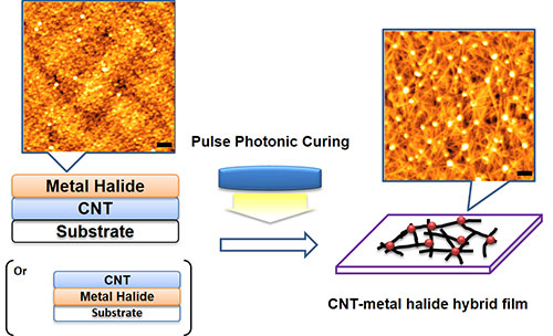 |
| Figure 1: The developed CNT transparent conductive film production process.
|
|
Atomic force microscope images of the CNT film before and after irradiation with pulsed light show that this irradiation causes nanoparticles of metal halide to grow and at the same time transfer to the interior of the CNT network. Moreover, after the irradiation with pulsed light, the nanoparticles are mainly located in places where two or more CNTs intersect with each other (Fig. 2). This indicates the possibility of enabling the CNT transparent conducting film to maintain high conductivity by the interconnecting-structured nanoparticles that reinforce the contacts between CNTs.
|
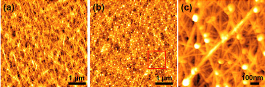 |
| Figure 2: Atomic force microscope images of CNT transparent conductive film. (a) CNT film without nanoparticles; (b) CNT film produced by the developed technology; (c) Enlarged image of (b).
|
|
Measurement of change in conductivity over time when the film is kept at room temperature in the open air shows that a conventional CNT transparent conductive film treated by nitric acid doping undergoes a rapid increase in sheet resistance immediately after it is produced, and sheet resistance continues to rise gradually after that. In contrast, the developed transparent conductive film maintains over a long period the same level of sheet resistance as it had immediately after it was produced (Fig. 3). This is because nanoparticles of metal halides do not volatilize even if exposed to the open air, so the film can maintain stable performance for a long period of time. The developed material represents an improvement of long-term stability of conductivity, which had been an obstacle to practical use of transparent conductive films that use CNTs or graphene in the past.
|
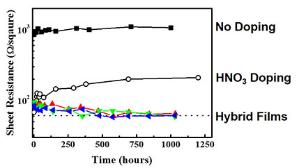 |
| Figure 3: Changes in sheet resistance of the developed CNT transparent conductive film over time.
|
|
Future Plans
|
|
The researchers aim to further improve the conductivity and transparency of CNT transparent conductive films by optimizing the type of nanoparticle material used and the conditions of optical processing. They also aim to produce such films using wet processes, such as coating and printing, for all processes. They further aim to use processes such as large-area patterning by screen printing to develop a wide range of applications in addition to touch panels, such as sensors, solar cell electrodes, and wearable electronics.
|

