(Nanowerk News) 'Whiskers' have been recorded in natural ores since the 1500s. These crystal formations indeed look like a cat’s whiskers, but function as wires. And since Bell Labs in the 1960s began to grow whiskers deliberately out of many different substances, materials scientists have been molding them into everything from photovoltaic devices, transistors, sensors, solid state lighting and batteries.
At IBM Research, with colleagues from academia and the Brookhaven National Laboratory, we have developed a way to make these structures grow in an electron microscope. By recording the atoms self-assembling to form the whiskers – renamed in modern fashion as nanowires – we hope to understand how they grow and how to tune the growth conditions to build nano-devices (Nature Materials, "Synthesis of nanostructures in nanowires using sequential catalyst reactions").
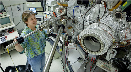
Dr. Frances Ross at the IBM Thomas J Watson Research Center. (Photo: Chris Ramirez for The New York Times)
The term nanowire describes any crystal that is thin in diameter, down to tens of nanometers, but with a length maybe hundreds or thousands of times greater. The material that the nanowire is made of, and its exact dimensions, determine its performance. For example, how solar energy is absorbed, in the case of photovoltaics. Or how lithium moves along a nanowire, in the case of rechargeable batteries. And how magnetic fields arrange themselves along its length, in the case of IBM’s racetrack memory. The big bang in these tiny structures comes from the fact that at nanoscale dimensions, even conventional materials can behave in remarkable and unexpected ways.
One exciting opportunity for nanowires is as building blocks for transistors in microelectronics. While getting to the 7 nanometer node is heroic, the lithographic process conventionally used to define the circuits is ultimately limited. Using self-assembled nanowires as the cores of the transistors can provide a pathway to smaller circuits, and perhaps even new designs that need less power to perform computations.
Our experiments started with the goal of understanding how the atoms spontaneously arrange themselves into the simplest sorts of nanowires, those that are made up of only one material. We chose our favorite element, silicon, the semiconductor that forms the basis of microelectronics. The nanowires grow with the help of a catalyst. So, we start with a flat wafer of silicon, add a couple of layers of gold atoms and heat until the gold and silicon react chemically and form tiny liquid droplets. The reaction takes place at 370°C, and results in something that looks a lot like a pane of glass covered by raindrops – at the nano-scale.
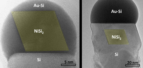
A silicon nanowire at 5nm and 20nm.
The trick is then to flow disilane gas, which contains silicon atoms, across the hot, droplet-covered silicon surface. When a molecule touches the surface of the silicon wafer, it bounces off and nothing changes. But when a molecule hits the surface of the gold droplet, it sticks and breaks apart, and its silicon atoms enter the droplet. As more silicon enters a droplet, the excess settles out as solid silicon beneath the droplet. Think of gradually adding spoonfuls of sugar to your coffee: excess sugar eventually settles at the bottom of the cup. In the case of the nanowires, the settling does not form disordered sludge, but instead a perfect layer of silicon atoms. The droplet stays at the top, and the nanowire keeps growing as long as we keep the gas flowing. The photo shows a nanowire during growth: the liquid droplet, labeled Au-Si, sits on top of the nanowire.
Watching this process in our electron microscope, and later in a microscope at Brookhaven National Laboratory with a high-speed (400 frames–per-second) movie camera, was an amazing experience. The video below shows the nanowire and the droplet, where the rows of dots indicate positions of silicon atoms in the nanowire. Layers of silicon atoms add onto the nanowire beneath the liquid droplet.
Watch how a silicon nanowire self-assembles under a gold-silicon droplet, and grows around a nanocrystal of nickel disilicide.
Droplet size determined the nanowire’s diameter. Temperature determined how long, and how quickly, the nanowire grew. We also tested other important semiconductors – germanium, gallium arsenide and gallium phosphide – and showed that their nanowires grew in a similar way. This finding helps us to understand how to build more complicated structures. So, we watched what happened as we switched from one gas to another, and learned the rules that govern which semiconductors could be stacked layer by layer, within a single nanowire.
Because each layer has different electronic behavior, these complicated nanowires could form versatile nano-devices. And it’s possible to grow even more complicated nanowires.
Our most recent experiments show what happens when we add metals, such as nickel or cobalt, to the catalytic droplet. Instead of settling out as a flat layer, the metal forms a single nanocrystal that floats in the droplet. Eventually this nanocrystal settles out, and we can grow the nanowire around it. This sequence of events was completely unexpected to us – imagine if you add that extra spoonful of sugar to your coffee and then find a perfect cube of sugar floating in the liquid! Electron microscope videos help us understand why the atoms assemble in this way, and how to control the resulting nanowire to optimize the shape, size and position of the embedded nanocrystals.
Self-assembling nanowires creates new concepts for nanomaterials, helping us build structures that cannot be fabricated using conventional techniques. The self-assembly process is still challenging because every nanowire comes out slightly different – perhaps imperfect for use in a device. We are not yet precise enough to exactly replicate the process across an entire wafer, much less build reliable nano-devices. However, each step forward, such as the nanowires with embedded nanocrystals, suggests new opportunities for electronics and other applications.
Self-assembly will succeed when we can harness the spontaneous behavior of atoms. That’s an exciting prospect. We need to change our way of thinking to avoid the need for perfection, but still control how the self-assembled structures behave under certain conditions – allowing us to create wholly unique devices and capabilities.
Source: By Dr. Frances Ross, materials scientist at IBM Research