| Posted: Sep 02, 2015 |
For 2-D boron, it's all about that base
(Nanowerk News) Rice University scientists have theoretically determined that the properties of atom-thick sheets of boron depend on where those atoms land.
|
|
Calculation of the atom-by-atom energies involved in creating a sheet of boron revealed that the metal substrate - the surface upon which two-dimensional materials are grown in a chemical vapor deposition (CVD) furnace - would make all the difference.
|
 |
| Rice University scientists have determined that still-theoretical two-dimensional boron would adjust its form depending on the substrate used in the growth process. They found that a copper substrate would be best for growing flat boron in a chemical vapor deposition furnace. (Image: Zhuzha Zhang/Rice University)
|
|
Theoretical physicist Boris Yakobson and his Rice colleagues found in previous work that CVD is probably the best way to make highly conductive 2-D boron and that gold or silver might be the best substrates.
|
|
But their new calculations show it may be possible to guide the formation of 2-D boron by tailoring boron-metal interactions. They discovered that copper, a common substrate in graphene growth, might be best to obtain flat boron, while other metals would guide the resulting material in their unique ways.
|
|
The Rice team's results appear today in the journal Angewandte Chemie ("Two-Dimensional Boron Monolayers Mediated by Metal Substrates").
|
|
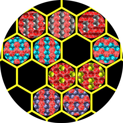
"If you make 2-D boron on copper, you get something different than if you made it on gold or silver or nickel," said Zhuhua Zhang, a Rice postdoctoral researcher and lead author of the paper. "In fact, you'd get a different material with each of those substrates."
|
|
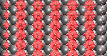
In chemical vapor deposition, heated gases deposit atoms on the substrate, where they ideally form a desired lattice. In graphene and boron nitride, atoms settle into flat hexagonal arrays regardless of the substrate. But boron, the researchers found, is the first known 2-D material that would vary its structure based on interactions with the substrate.
|
|
Perfectly flat boron would be a grid of triangles with occasional hexagons where atoms are missing. The researchers ran calculations on more than 300 boron-metal combinations. They found the pattern of atoms in a copper surface match up nicely with 2-D boron and the strength of their interactions would help keep the boron flat. A nickel substrate would work nearly as well, they found.
|
 |
| Two-dimensional boron would take a different forms, depending on the substrate used in chemical vapor deposition growth, according to Rice University researchers. (Image: Zhuzha Zhang/Rice University)
|
|
On gold and silver, they determined weak atomic interactions would allow the boron to buckle. In an extension, they theorized that naturally forming, 12-atom icosahedrons of boron would assemble into interconnected sheets on copper and nickel, if the boron supply were high enough.
|
|
One remaining downside to 2-D boron is that, unlike graphene, it will remain difficult to separate from its substrate, which is necessary for use in applications.
|
|
But that strong adhesion may have a side benefit. Further calculations suggested boron on gold or nickel may rival platinum as a catalyst for hydrogen evolution reactions in applications like fuel cells.
|
|
"In 2007 we predicted the possibility of pure boron fullerenes," Yakobson said. "Seven years later, the first one was observed in a laboratory. This time, with the enormous attention researchers are giving to 2-D materials, I'd hope some lab around the world will make 2-D boron much sooner."
|

