| Posted: Oct 20, 2015 |
Researchers demonstrate atomically thin excitonic laser
(Nanowerk News) An important step towards next-generation ultra-compact photonic and optoelectronic devices has been taken with the realization of a two-dimensional excitonic laser. Scientists with the U.S. Department of Energy (DOE)'s Lawrence Berkeley National Laboratory (Berkeley Lab) embedded a monolayer of tungsten disulfide into a special microdisk resonator to achieve bright excitonic lasing at visible light wavelengths.
|
|
"Our observation of high-quality excitonic lasing from a single molecular layer of tungsten disulfide marks a major step towards two-dimensional on-chip optoelectronics for high-performance optical communication and computing applications," says Xiang Zhang, director of Berkeley Lab's Materials Sciences Division and the leader of this study.
|
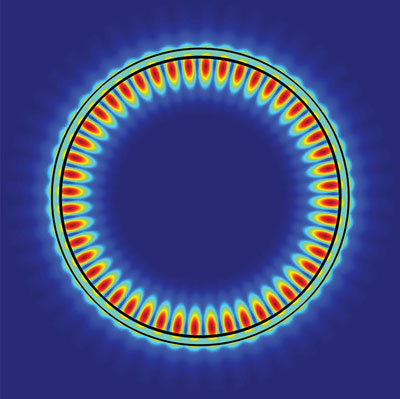 |
| In the whispering gallery mode of a 2D excitonic laser made from a monolayer of tungsten disulfide and a microdisk resonator, the electric field at the edges of the resonator helps promote a high Q factor with low power consumption.
|
|
Zhang, who also holds the Ernest S. Kuh Endowed Chair at the University of California (UC) Berkeley and is a member of the Kavli Energy NanoSciences Institute at Berkeley (Kavli ENSI), is the corresponding author of a paper describing this research in the journal Nature Photonics ("Monolayer excitonic laser"). The paper is titled "Monolayer excitonic laser." The lead authors are Yu Ye and Zi Jing Wong, members of Zhang's research group, plus Xiufang Lu, Xingjie Ni, Hanyu Zhu, Xianhui Chen and Yuan Wang.
|
|
Among the most talked about class of materials in the world of nanotechnology today are two-dimensional (2D) transition metal dichalcogenides (TMDCs). These 2D semiconductors offer superior energy efficiency and conduct electrons much faster than silicon. Furthermore, unlike graphene, the other highly touted 2D semiconductor, TMDCs have natural bandgaps that allow their electrical conductance to be switched "on and off," making them more device-ready than graphene. Tungsten disulfide in a single molecular layer is widely regarded as one of the most promising TMDCs for photonic and optoelectronic applications. However, until now, coherent light emission, or lasing, considered essential for "on-chip" applications, had not been realized in this material.
|
|
"TMDCs have shown exceptionally strong light-matter interactions that result in extraordinary excitonic properties," Zhang says. "These properties arise from the quantum confinement and crystal symmetry effect on the electronic band structure as the material is thinned down to a monolayer. However, for 2D lasing, the design and fabrication of microcavities that provide a high optical mode confinement factor and high quality, or Q, factor is required."
|
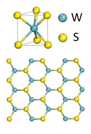 |
| A single molecular layer of tungsten (W) and sulfide (S) is widely regarded as one of the most promising 2D semiconductors for photonic and optoelectronic applications.
|
|
In a previous study, Zhang and his research group had developed a "whispering gallery microcavity" for plasmons, electromagnetic waves that roll across the surfaces of metals. Based on the principle behind whispering galleries - where words spoken softly beneath a domed ceiling can be clearly heard on the opposite side of the chamber - this micro-sized metallic cavity for plasmons strengthened and greatly enhanced the Q factor of light emissions. In this new study, Zhang and his group were able to adapt this microcavity technology from plasmons to excitons - photoexcited electrons/hole pairs within a single layer of molecules.
|
|
"For our excitonic laser, we dropped the metal coating and designed a microdisk resonator that supports a dielectric whispering gallery mode rather than a plasmonic mode, and gives us a high Q factor with low power consumption," says co-lead author Ye. "When a monolayer of tungsten disulfide - serving as the gain medium - is sandwiched between the two dielectric layers of the resonator, we create the potential for ultralow-threshold lasing."
|
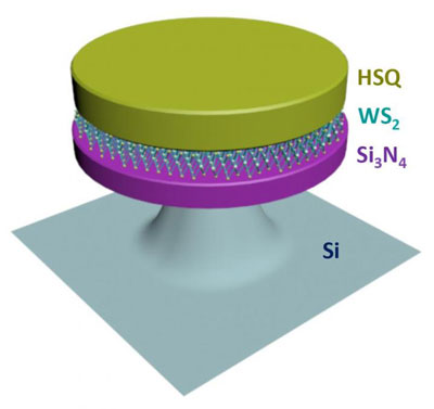 |
| In this 2-D excitonic laser, the sandwiching of a monolayer of tungsten disulfide between the two dielectric layers of a microdisk resonator creates the potential for ultralow-threshold lasing. (Image: Xiang Zhang, Berkeley Lab)
|
|
In addition to its photonic and optoelectronic applications, this 2D excitonic laser technology also has potential for valleytronic applications, in which digital information is encoded in the spin and momentum of an electron moving through a crystal lattice as a wave with energy peaks and valleys. Valleytronics is seen as an alternative to spintronics for quantum computing.
|
|
"TMDCs such as tungsten disulfide provide unique access to spin and valley degrees of freedom," says co-lead author Wong. "Selective excitation of the carrier population in one set of two distinct valleys can further lead to lasing in the confined valley, paving the way for easily-tunable circularly polarized lasers. The demand for circularly polarized coherent light sources is high, ranging from three-dimensional displays to effective spin sources in spintronics, and information carriers in quantum computation."
|

