| Posted: Jun 19, 2016 |
Change an atom, change a material
(Nanowerk News) With just the change of an atom, researchers using two U.S. Department of Energy synchrotron light sources, including the Advanced Photon Source (APS) at Argonne, have found it is possible to change a material’s properties. As modern technology demands components that fit into smaller spaces, research like theirs plays a valuable role in making that possible. The results, published in the Proceedings of the National Academy of Sciences ("Atomic-scale control of magnetic anisotropy via novel spin–orbit coupling effect in La2/3Sr1/3MnO3/SrIrO3 superlattices"), reveal a novel magnetic state that could pave the way for new devices.
|
|
Understanding this discovery starts with the electrons: particularly how they spin (spin, like charge, is a fundamental property of an electron). The difference is that spin has directionality as a vector. Researchers have to use an electric field to control charge and a magnetic field to orient spin.
|
|
The exception is when an electron is on the move.
|
|
Einstein’s relativity tells us that the spin of an electron “sees” its own charge motion – the electron orbit. Or, conversely, the charge “knows” the spin direction as soon as it moves. The orbital provides a channel for the two properties to interact and affect each other. This is very much like the way one adds some spin to a ball to control its trajectory, such as in football, baseball, and basketball.
|
|
This phenomenon is called spin-orbit coupling (SOC) and plays a key role in the this study. Spintronics is a growing field of interest with the goal of using electron spin for devices. This requires controlling the magnetism. Several studies in this vein have featured different transition metal oxides (TMOs), but there have been limits to their potential. Some materials, for example, are ferromagnetic but have weak spin-orbit coupling, while others have stronger SOC but the correlation strength isn’t strong enough to host magnetism. These researchers had as their objective the best of both worlds.
|
 |
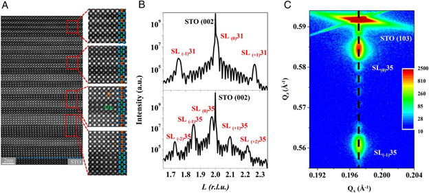
| Fig. 1. Structural characterization of the LSMO/SIO superlattice. (A) High-angle annular dark-field (HAADF) STEM images of LSMO/SIO superlattice with designed periodicities in one sample. The four high-magnification images correspond to the regions of (LSMO)1/(SIO)1, (LSMO)2/(SIO)2, (LSMO)3/(SIO)3, and (LSMO)5/(SIO)5 from top to bottom (the number refers to the thickness in uc). The atoms are marked by different colors: Ir (brightest contrast) in orange, Mn (darkest contrast) in green, and A-site atoms in blue. (B) θ-2θ X-ray diffractograms of an SL31 (Top) and an SL35 (Bottom) superlattice. Both the superlattice peaks and the thickness fringes reveal the high degree of interface abruptness. (C) X-ray reciprocal spacing mapping of an SL35 superlattice around (103) peak, confirming coherent growth of the superlattice. (click on image to enlarge)
|
|
To achieve the best magnetic state, these researchers from the University of California, Berkeley; the University of Tennessee; Lawrence Berkeley National Laboratory; and Argonne combined two materials. One was ferromagnetic and comprised lanthanum, strontium, manganese, and oxygen (LSMO). The second was paramagnetic and was made from strontium, iridium, and oxygen (SIO). They grew layers of the materials on top of one another in a specific pattern.
|
|
Normally, to create or grow a three-dimensional crystal, one would keep piling up these layers. Here, the team grew LSMO and stopped the piling process after every three layers, laid down one layer of SIO, and resumed the piling for LSMO. In the end they had a LSMO crystal with intercalated SIO layers. One can think of it as sliding in thin layers of ham into a long breadstick with equal spacing, and turning it into a super-sandwich.
|
|
The material was characterized (Fig.1) using x-ray absorption spectroscopy (XAS) and X-ray magnetic circular dichroism (XMCD) of the magnesium edge at beamline 4.0.2 at the Advanced Light Source (ALS, Lawrence Berkeley National Laboratory; XAS and XMCD characterizations at the iridium edge were performed at X-ray Science Division (XSD) beamline 4-ID-D of the APS, while x-ray diffraction measurements were carried out at the XSD 33-BM-C and 6-ID-B beamlines of the APS (both the APS and ALS are Office of Science user facilities).
|
|
A critical step was tuning the layer dimensions. Building the sandwich (or superlattice) as they did scaled-down the SIO layer to 0.4 nanometer. This confinement allowed for manipulation of the magnetism, owing to a novel spin-orbit coupling state that developed in the SIO layers. Those results wouldn’t have been possible without precise control—at the atomic level—of the SIO thickness.
|
|
Tuning the layer size causes something that would not happen in each individual material. The bread and the ham would never taste the same as the sandwich.
|
|
The benefits of controlling magnetism at the atomic scale continue to grow with the demand for more sophisticated devices.
|
|
As modern technology develops, we want to make everything small and fit more processors, more memories, and more circuits into a small space. There is nothing better than being able to design your material property and device function with just a change of an atom, which is exactly what we achieve. The researchers replaced one atomic plane of manganese with iridium, and the magnetization pointed to a different direction.
|
|
The possibilities of engineering at this scale could also open doors for all-oxide spintronics. Modern magnetic devices rely on metals and alloys, but they can be unstable in an oxidizing environment, which isn’t a problem for oxides. Moreover, oxides have functionalities that metals lack, such as high-temperature superconductivity and ferroelectrcity.
|
|
An all oxide platform allows integrating these materials for multifunctional devices.
|
|
The authors note that to their knowledge, this research represents the first experimental studies of this type of superlattice and the effects of dimensional confinement. The work also showed that non-magnetic materials can be used to engineer magnetic materials if they’re matched with the right partner in the appropriate geometry. It is possible other combinations of this type might have the same effect. While the possibility of finding materials for spintronic devices is exciting, the physics itself is equally interesting for scientists. In this case, they found unexpected magnetism from the quantum entanglement of two different spin-orbits.
|
|
“This means that the electron can exist in two different orbits simultaneously and its spin can point to opposite direction at the same time,” said article co-author Jian Liu of the University of Tennessee. “One cannot imagine how to throw the same football along two trajectories with different spinning motions at the same time. Quantum mechanics is just fascinating.”
|