| Nov 01, 2018 |
Atoms use tunnels to escape graphene cover(Nanowerk News) Graphene has held a great promise for applications since it was first isolated in 2004. But we still don’t use it in our large-scale technology, because we have no way of producing graphene on an industrial scale. |
| Leiden physicists have now visualized for the first time how atoms behave in between graphene and a substrate (Physical Review Materials, "Intrinsic stacking domains in graphene on silicon carbide: A pathway for intercalation"). This insight could be instrumental for future implementations of industrial graphene production. |
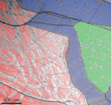 |
| LEEM image of a graphene layer grown on a silicon carbide substrate. A red color indicates the presence of hydrogen atoms sandwiched between graphene and silicon carbide. The dark lines indicate strained regions in the graphene. The surrounding white areas show where the hydrogen atoms already left the interface. This shows that the lines act as tunnels where the hydrogen flows away faster. (Image: Leiden University) |
| In 2004, scientists managed to isolate a single layer of carbon atoms from a block of graphite. Since then, this so-called graphene layer has been praised for its high potential for all sorts of promising applications. It would enable high-speed transistors, economic electrical cars and delicate sensors. |
| So fast-forward to 2018, graphene is now the dominant building block of our computers, cars and gadgets, right? Wrong. There are still few large-scale graphene applications. The problem is that we haven’t figured out a way to produce graphene in high quality on the right substrate on an industrial scale. |
Hydrogen atoms |
| Though scientists do have an idea for large-scale production. If they heat silicon carbide to almost 2,000 °C, a graphene layer grows on its surface. However, they need to make sure that the desired properties of the graphene are not disturbed by the substrate. |
| Inserting hydrogen atoms in between the graphene and silicon carbide isolates the graphene and leaves it intact as a single layer material. |
| Leiden physicist Sense Jan van der Molen and his research group have now visualized for the first time how those atoms behave underneath the graphene. |
Strained |
| The researchers, including postdoc Johannes Jobst and PhD candidate Tobias de Jong, used their Low-Energy Electron Microscope (LEEM) to study what happens to hydrogen atoms sandwiched between graphene and silicon carbide. They spotted lines where the graphene layer is strained. |
| The hydrogen atoms use the lines as tunnels where they can escape more easily, whereas they stay put much longer under the graphene’s smooth regions between these lines. |
| ‘The reversed process is widely used in research to decouple the graphene from the substrate,’ says Jobst. ‘But it was not clear how the hydrogen moves at the interface. We showed that hydrogen gas can be blown into those tunnels so that it will spread quickly underneath the graphene layer in the form of individual atoms.’ |
| Source: Leiden University |
|
Subscribe to a free copy of one of our daily Nanowerk Newsletter Email Digests with a compilation of all of the day's news. |

