| May 21, 2019 |
Mathematical technique quickly tunes next-generation lenses(Nanowerk News) Most of us know optical lenses as curved, transparent pieces of plastic or glass, designed to focus light for microscopes, spectacles, cameras, and more. For the most part, a lens’ curved shape has not changed much since it was invented many centuries ago. |
| In the last decade, however, engineers have created flat, ultrathin materials called metasurfaces that can perform tricks of light far beyond what traditional curved lenses can do. Engineers etch individual features, hundreds of times smaller than the width of a single human hair, onto these metasurfaces to create patterns that enable the surface as a whole to scatter light very precisely. But the challenge is to know exactly what pattern is needed to produce a desired optical effect. |
| That’s where MIT mathematicians have come up with a solution. In a study published in Optics Express ("Topology optimization of freeform large-area metasurfaces"), a team reports a new computational technique that quickly determines the ideal makeup and arrangement of millions of individual, microscopic features on a metasurface, to generate a flat lens that manipulates light in a specified way. |
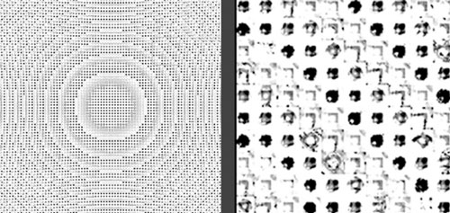 |
| MIT mathematicians have developed a technique that quickly determines the ideal arrangement of millions of individual, microscopic features on a metasurface, to generate a flat lens that manipulates light in a specified way. The team designed a metasurface, at left, etched with millions of features. A zoomed-in image of the lens, right, shows individual features, each etched in a specific way so that, together, they produce a desired optical effect. (Image: Zin LIn) |
| Previous work attacked the problem by limiting the possible patterns to combinations of predetermined shapes, such as circular holes with different radii, but this approach only explores a tiny fraction of the patterns that can potentially be made. |
| The new technique is the first to efficiently design completely arbitrary patterns for large-scale optical metasurfaces, measuring about 1 square centimeter — a relatively vast area, considering each individual feature is no more than 20 nanometers wide. Steven Johnson, professor of mathematics at MIT, says the computational technique can quickly map out patterns for a range of desired optical effects. |
| “Say you want a lens that works well for several different colors, or you want to take light and instead of focusing it to a spot, make a beam or some sort of hologram or optical trap,” Johnson says. “You can tell us what you want to do, and this technique can come up with the pattern that you should make.” |
Pixel-by-pixel |
| A single metasurface is typically divided into tiny, nanometer-sized pixels. Each pixel can either be etched or left untouched. Those that are etched can be put together to form any number of different patterns. |
| To date, researchers have developed computer programs to search out any possible pixel pattern for small optical devices measuring tens of micrometers across. Such tiny, precise structures can be used to, for instance, trap and direct light in an ultrasmall laser. The programs that determine the exact patterns of these small devices do so by solving Maxwell’s equations — a set of fundamental equations that describe the scattering of light — based on every single pixel in a device, then tuning the pattern, pixel by pixel, until the structure produces the desired optical effect. |
| But Johnson says this pixel-by-pixel simulation task becomes nearly impossible for large-scale surfaces measuring millimeters or centimeters across. A computer would not only have to work with a much larger surface area, with orders of magnitude more pixels, but also would have to run multiple simulations of many possible pixel arrangements to eventually arrive at an optimal pattern. |
| “You have to simulate on a scale big enough to capture the whole structure, but small enough to capture fine details,” Johnson says. “The combination is really a huge computational problem if you attack it directly. If you threw the biggest supercomputer on Earth at it, and you had a lot of time, you could maybe simulate one of these patterns. But it would be a tour de force.” |
An uphill search |
| Johnson’s team has now come up with a shortcut that efficiently simulates the desired pattern of pixels for large-scale metasurfaces. Instead of having to solve Maxwell’s equations for every single nanometer-sized pixel in a square centimeter of material, the researchers solved these equations for pixel “patches.” |
| The computer simulation they developed starts with a square centimeter of randomly etched, nanometer-sized pixels. They divided the surface into groups of pixels, or patches, and used Maxwell’s equations to predict how each patch scatters light. They then found a way to approximately “stitch” the patch solutions together, to determine how light scatters across the entire, randomly etched surface. |
| From this starting pattern, the researchers then adapted a mathematical technique known as topology optimization, to essentially tweak the pattern of each patch over many iterations, until the final, overall surface, or topology, scatters light in a preferred way. |
| Johnson likens the approach to attempting to find your way up a hill, blindfolded. To produce a desired optical effect, each pixel in a patch should have an optimal etched pattern that should be attained, that could be thought of metaphorically as a peak. Finding this peak, for every pixel in a patch, is considered a topology optimization problem. |
| “For each simulation, we’re finding which way to tweak each pixel,” Johnson says. “You then have a new structure which you can resimulate, and you keep doing this process, each time going uphill until you reach a peak, or optimized pattern.” |
| The team’s technique is able to identify an optimal pattern in just a few hours, compared with traditional pixel-by-pixel approaches which, if applied directly to large metasurfaces, would be virtually intractable. |
| Using their technique, the researchers quickly came up with optical patterns for several “metadevices,” or lenses with varying optical properties, including a solar concentrator that takes incoming light from any direction and focuses it to a single point, and an achromatic lens, which scatters light of different wavelengths, or colors, to the same point, with equal focus. |
| “If you have a lens in a camera, if it’s focused on you, it should be focused for all colors simultaneously,” Johnson says. “The red shouldn’t be in focus but the blue out of focus. So you have to come up with a pattern that scatters all the colors in the same way so they go into the same spot. And our technique is able to come up with a crazy pattern that does that.” |
| Going forward, the researchers are working with engineers, who can fabricate the intricate patterns that their technique maps out, to produce large metasurfaces, potentially for more precise cellphone lenses and other optical applications. |
| “These surfaces could be produced as sensors for cars that drive themselves, or augmented reality, where you need good optics,” Pestourie says. “This technique allows you to tackle much more challenging optical designs.” |
| Source: By Jennifer Chu, MIT |
|
Subscribe to a free copy of one of our daily Nanowerk Newsletter Email Digests with a compilation of all of the day's news. |

