| Jun 04, 2019 |
UV light may illuminate improvements for next generation electronic devices(Nanowerk News) By adding one more layer of atoms to already infinitesimal semiconductors, a next-level generation of electrical devices becomes possible. This work to build better and faster electronics is well underway, but little was known about how to test the ingredients of these devices to ensure performance. |
| Now, researchers from the Nagoya Institute of Technology (NITech) in Japan have developed a method to make sure the connections between the two-dimensional layer of atoms and the semiconductors are as perfect as possible. |
| The researchers published their results in Applied Physics Letters ("Ultraviolet light induced electrical hysteresis effect in graphene-GaN heterojunction"). |
| They applied a layer of graphene to gallium nitride, a commonly used semiconductor. The graphene is made of a single layer of atoms, while the gallium nitride is a three-dimensional structure. Together, graphene and gallium nitride are known as a heterojunction device, with significant sensitivity to the interface properties of metal and semiconductors. |
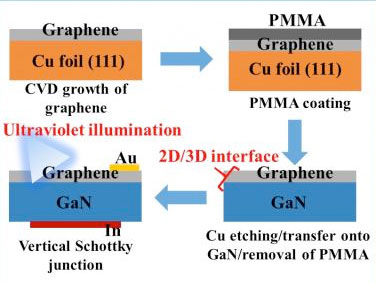 |
| Determining the graphene-GaN heterojunction interface under ultraviolet illumination. Researchers of the study shows the fabrication process of vertical Schottky junction with monolayer graphene on free-standing GaN. (Image: Golap Kalita, Ph.D., Nagoya Institute of Technology) |
| According to Golap Kalita Ph.D., an associate professor at NITech, understanding GaN heterojunction devices and how to improve them is critical for better device performance. |
| "Our team found a way to determine the interface properties of the graphene and gallium nitride heterojunction by characterizing the device under ultraviolet illumination," Kalita said. |
| The interface between the graphene and the gallium nitride should be free of impurities, especially ones that gain energy from light. When the researchers shined ultraviolet (UV) light on the heterojunction device, they found photo-excited electrons (excitons) trapped at the interface and interfering with the transfer of information. |
| The gallium nitride contains surface-level defects and other imperfections that allow such photo-excited electrons to become trapped at the interface. |
| "We found that the interface states of graphene and gallium nitride have a significant influence on the junction behavior and device properties," Kalita said. |
| One such property is called electrical hysteresis - it is a phenomenon in which electrons get trapped at the interface leading to behavioral shift in the device. The trapping of electrons is extremely sensitive to UV light. It means that once the UV light is shined on the heterojunction, the excited electrons get populated at the interface and remain as trapped, creating large hysteresis window. |
| However, when the researchers applied a more refined layer of graphene to gallium nitride, they didn't see any the hysteresis effect without light illumination, implying a cleaner match at the interface. But it wasn't perfect -- UV illumination instigated the photo-excited electrons into a frenzy behavior due to inherent defects in gallium nitride. |
| "This finding showed that the graphene/GaN heterojunction interface can be evaluated by the ultraviolet illumination process," Kalita said. |
| The ability to evaluate the purity of the interface is invaluable in the development of high-performance devices, according to the researchers. |
| "This study will open up new possibilities to characterize other heterojunction interfaces by an ultraviolet light illumination process," Kalita said. "Ultimately, our goal is to understand interface of various two- and three-dimensional heterostructures to develop novel optoelectronic devices with graphene." |
| Source: Nagoya Institute of Technology |
|
Subscribe to a free copy of one of our daily Nanowerk Newsletter Email Digests with a compilation of all of the day's news. |

