| Aug 06, 2019 |
A modified device fabrication process achieves enhanced spin transport in graphene(Nanowerk News) Spintronics is a field of research that was born in the 1980s. It amplifies the potential of traditional electronics by exploiting the electron’s spin degree of freedom, in addition to the usual state of charge. In the end, the goal is the same: to obtain devices to store, process and read information, but with enhanced characteristics such as lower power consumption, less heat dissipation, higher speed, etc. |
| Although spintronics has not yet become as widespread as its conventional predecessor, some current devices are based on this new approach, such as magnetic hard disks, magnetic random access memories and magnetic sensors with varied applications in industrial environments, robotics and automotive industry. |
| Graphene is a promising material in this field. Spins can flow efficiently in it over long distances, meaning that they do not change their state (let’s say, from “up” to “down”) for a relatively long time. Due to its large-scale production, CVD graphene is becoming popular to fabricate spintronic devices. However, impurities arising from the graphene growth and device fabrication process limit its performance. |
| A team of scientists from the ICN2 Physics and Engineering of Nanodevices Group, led by ICREA Prof. Sergio O. Valenzuela, has proposed a high-yield device fabrication process from CVD graphene that has improved substantially its spin parameters. The work, whose first author is Zewdu M. Gebeyehu, was fruit of a collaboration with Imec and K.U. Leuven (Belgium). The results have been published in 2D Materials ("Spin communication over 30 µm long channels of chemical vapor deposited graphene on SiO2"). |
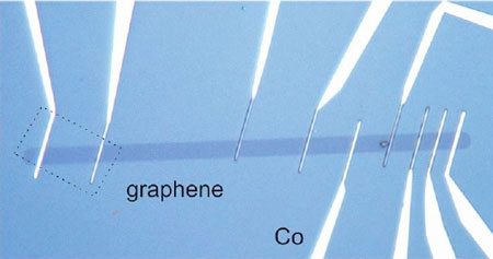 |
| Monolayer graphene on SiO2/Si substrates. |
| They demonstrate a spin signal measured across a 30 µm long channel with room-temperature spin lifetimes of up to 3 ns and spin relaxation lengths of up to 9 µm in monolayer graphene on SiO2/Si substrates. These spin parameters are the highest values for any form of graphene (both exfoliated and CVD graphene) on a standard SiO2/Si substrate. |
| To achieve this enhanced spin performance, the researchers used CVD graphene grown on a platinum foil and they modified the device fabrication technique so as to reduce the impurity levels associated with the graphene growth and fabrication steps. |
| The latter requires the optimization of several standard processes, involving the preselection of high-quality uniform graphene with low level of impurities, an etching step combining e-beam lithography and oxygen plasma and a suitable post-annealing in high vacuum. The approach can be scaled and allows a highly reproducible fabrication of devices, which is the main requirement for potential industrialization. |
| The improvement on the spin parameters together with the reproducibility of the device fabrication process brings us closer to the realization of complex circuit architectures for spintronic devices such as spin logic and logic-in-memory for beyond CMOS computing. |
| Source: Catalan Institute of Nanoscience and Nanotechnology |
|
Subscribe to a free copy of one of our daily Nanowerk Newsletter Email Digests with a compilation of all of the day's news. |

