| Dec 16, 2019 |
Looking inside 3D silicon nanostructures without leaving a trace: 'the Good, the Bad, the Ugly'(Nanowerk News) Scientists from the University of Twente and the European Synchrotron Radiation Facility in France have discovered a new method to non-destructively look inside three-dimensional (3D) nanostructures without breaking them. |
| The study is timely since 3D nanostructures are drawing a fast-growing attention for their advanced functionalities in nanophotonics, photovoltaics, 3D integrated circuits, and flash memories (see for instance: "How to gather many merry people at a party?" and "A prison for photons in a diamond-like photonic crystal"). |
| The traditional way to look inside 3D nanostructures is to cut them from their substrate, or slice them and view each slice separately. |
| The new method allows to view the complete 3D structure of the whole nanodevice without cutting or breaking. Hence the traceless method allows to use the device further after the 3D image was made. |
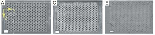 |
| Figure 1. Electron microscope images of three 3D photonic crystal nanostructures fabricated in the same way. Each external surface looks closely matches the design and looks like the other, but the functionality and internal structure will appear to be completely different. |
| The breakthrough results just appeared in the leading journal ACS Nano ("X-Ray Imaging of Functional Three-Dimensional Nanostructures on Massive Substrates"). |
| The world around us is truly three-dimensional. As a child you learn that you do not want to break things when checking out your surroundings. The same holds for scientists: once you manage to fabricate a new experimental sample, you do not want to destroy it while investigating whether it indeed behaves as expected. This holds even more so in the wonderful world of nanotechnology where functional properties of nanostructures are essentially defined by the 3D arrangement of material inside. |
| Therefore, nanotechnologists carefully design 3D nanostructures to achieve a specific functionality. And in real life, new samples never match the initial design perfectly, so it is crucial to investigate what your sample turned out to be. |
| A simple approach to figure out if your fabricated nanostructure matches the design, is to study it under the microscope. To illustrate the challenges in such an approach let us consider the following quiz: Let us consider three samples shown in Fig. 1 that are fabricated in the same way. Can you tell by the appearance in the electron microscope images, whether they are indeed the same inside and have the same functionality? |
| Obviously, a microscope image only gives information about the outside of the sample, whereas know-how of the internal structure is needed. Traditionally, this challenge is solved by slicing the sample into thin layers and studying the layers one by one to learn about the internal structure. Such popular, yet destructive methods have an obvious disadvantage: one may find that the sample was made according to specifications, but alas, it is then destroyed. |
| Suitable ways to view inside 3D structures are X-ray methods. But even in recent X-ray work, samples were typically cut out from the device or substrate to achieve sufficient transmission and contrast. |
| In their new paper, the team demonstrates ???traceless X-ray tomography??? (TXT). One major step forward is the much greater feasible thickness of the sample of more than a millimeter of silicon, due to the much higher X-ray photon energy. |
| Grishina enthuses: ???In modern nanotechnology this is plenty sufficient to image through wafers. Indeed, all silicon device remained untouched and ???as is??? during the study.??? |
| Moreover, the team???s method greatly improved the total sample size to field-of-view ratio, allowing to zoom-in on the desired region. |
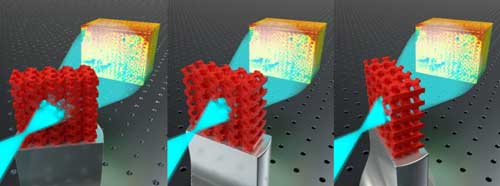 |
| Figure 2. Animation sequence showing that TXT data are recorded while rotating the sample (three orientations are shown). From the recorded radiographs, the tomographic reconstruction is derived that is shown in the background. |
| Holographic tomography experiments were performed at the European Synchrotron Radiation Facility (ESRF). The hard X-ray beam with 17 keV photon energy propagates in the z-direction and is focused with multilayer coated Kirkpatrick-Baez optics to a tiny, 23 nm x 37 nm, focus. |
| Cloetens explains: ???One key feature of our TXT study is the use of X-rays with a much higher photon energy than before. Therefore, the attenuation length for silicon is 640 µm, which is 9 to 20?? greater than before, and sufficient to traverse wafer-thick silicon substrates.??? |
| The sample is placed at a small distance downstream from the focus and the detector is placed further downstream. At each distance, 1500 images were recorded while rotating the sample about the Y???axis as shown in Figure 2. The data processing is an intensive two-step procedure consisting of a phase retrieval step followed by a tomographic reconstruction. |
 |
| Figure 3. Birds-eye view of reconstructed 3D silicon nanostructures shown in the SEM images in Fig. 1. (A) 3D photonic crystal that reveals a broad photonic gap in agreement with theory: ???the Good???. (B) 3D photonic crystal that reveals a large void due to stiction resulting from violent liquid evaporation in the pores: ???the Bad???. (C) Sample that shows shallow pores due to a fabrication error: ???the Ugly???. The nicknames are inspired by a fa??mous ???spaghetti western???. (click on image to enlarge) |
| The team studied exemplary 3D photonic band gap crystals made from silicon by CMOS-compatible means (a breakthrough a few years ago.) They obtained real space 3D density distributions with 55 nm spatial resolution. |
| TXT identifies why nanostructures that look similar in electron microscopy (see Figure 1) have vastly different nano??photonic functionality: One "Good" crystal with a broad photonic gap reveals 3D periodicity as designed (see Figure 3), a second "Bad" structure without gap reveals a buried void, a third "Ugly" one without gap is shallow due to errors during the fabrication. |
| Vos explains: ???TXT serves to non-destructively differentiate between the possible reasons of not finding the designed and expected performance. This is why we think that TXT is an original and powerful tool to critically assess 3D functional nanostructures. Judging from responses at conferences, it seems that our colleagues agree. Or is it perhaps because they like spaghetti-Western movies???? |
| Source: University of Twente |
|
Subscribe to a free copy of one of our daily Nanowerk Newsletter Email Digests with a compilation of all of the day's news. |

