| Feb 05, 2020 |
Building upon carbon nanotubes to create a novel functional structure(Nanowerk News) For decades, carbon nanotubes held great promise of developments in the field of electronics and more. But one drawback to realizing these innovations has been the difficulty of incorporating additional materials into nanotubes. |
| For the first time, researchers have grown crystals of various materials uniformly onto the surface of carbon nanotubes (Science, "One-dimensional van der Waals heterostructures"). They hope these modified structures will exhibit functions useful in electronic, chemical or other applications. |
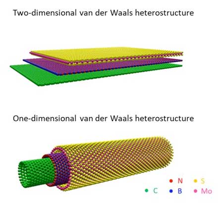 |
| A visual comparison of 2D (above) and 1D (below) vdWs. (© Science) |
| We all know that as technology progresses, devices become ever smaller and more feature laden. Such advancements are possible due to the continued work of scientists who explore new ways of coaxing materials to perform useful functions. One area researchers eagerly investigate is the function of flat two-dimensional (2D) crystals, each just one molecule thick. These are arranged in layers to create structures called van der Waals heterostructures (vdWs). |
| "Many interesting phenomena have been seen in 2D vdWs and new kinds of electronic and optical components have been proposed as a result," said Professor Shigeo Maruyama. "However, we wondered whether it's possible to create spatially compact one-dimensional (1D) vdWs and what kinds of useful and unique properties these nanotube structures may have." |
| It turns out 1D vdWs are possible to fabricate, but it's far from easy. Maruyama, Associate Professor Rong Xiang and their team first created some pure carbon (C) nanotubes, which in itself is still a relatively new and difficult process. These were placed in a high-temperature atmosphere containing boron nitride (BN), which binds to the surface of the nanotube to form a uniform and continuous layer or crystal. |
| A similar process then adds a third layer to this tube in the form of molybdenum disulfide (MoS2). When tube structures encapsulate one another like this it's called a coaxial structure, as multiple 1D shapes share an axis of orientation. |
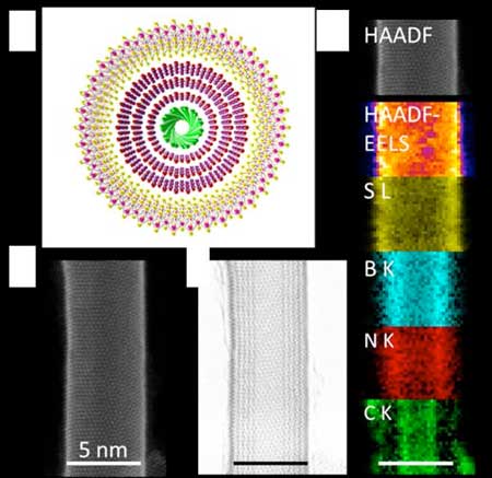 |
| Microscopic images of the 1D vdW taken by various instruments. (© Science) |
| "At that time, the yield of this structure was still extremely low. I spent one full day at the controls of a transmission electron microscope probing the sample," explained Xiang. "In the afternoon when I was almost giving up, I found one of our coaxial nanotubes. Then a few minutes later, I found a second one! With two observations, I become fully confident that MoS2 based 1D vdWs can exist." |
| 1D vdWs are an entirely new class of material and its properties have not yet been studied. But Maruyama, Xiang and their team are hopeful that these interesting structures may find use in applications such as flexible electronics, lasers, solar energy conversion, electrocatalytic water splitting (to produce hydrogen), photoelectric devices and more. |
| Source: University of Tokyo |
|
Subscribe to a free copy of one of our daily Nanowerk Newsletter Email Digests with a compilation of all of the day's news. |

