| Apr 27, 2020 |
Synthesis of silicon intercalated monolayer blue phosphorus(Nanowerk News) National University of Singapore (NUS) chemists have developed a method to synthetically produce monolayer blue phosphorus for potential semiconductor applications (ACS Nano, "Synthesis of monolayer blue phosphorus enabled by silicon intercalation"). |
| The ability to design and produce materials synthetically could complement the library of naturally occurring layered solids and provide opportunities to develop new materials with unique properties suited for specialised applications. |
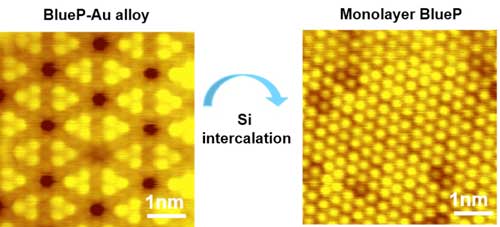 |
| (Left) Figure shows the scanning tunnelling microscopy (STM) image of blue phosphorus-gold (BlueP-Au) alloy grown on gold (111) substrate. (Right) Figure shows the STM image of the single layer blue phosphorus (BlueP). The structure is not completely flat but regularly buckled. (© ACS Nano) |
| The class of two-dimensional (2D) elemental materials is particularly interesting as they represent the chemically simplest case for materials development, and serve as a model system for exploring on-surface synthesis mechanisms. One such 2D materials is blue phosphorus, which has been calculated to possess a large band gap suitable for use in optoelectronic devices. |
| A research team led by Prof CHEN Wei from the Department of Chemistry and Department of Physics, NUS has demonstrated experimentally that an atomically-thin layer of pure blue phosphorus can be obtained from silicon intercalation of a blue phosphorus-gold (BlueP-Au) alloy. A single layer of BlueP-Au alloy was prepared by depositing bulk black phosphorus precursors onto a heated gold (111) surface. Silicon molecules were subsequently evaporated from a heated silicon rod. These silicon atoms inserted themselves below the BlueP-Au alloy and formed a gold silicide buffer layer, breaking the molecular bonds between the phosphorus and gold atoms, thereby leading to the formation of a pure single layer of blue phosphorus on the surface. |
| Prof Chen said, “Future research work would be directed towards the isolation of the blue phosphorus monolayer from the substrate to study its performance in electronic devices. We also envisage that our findings will provide insights on the essential roles played by the substrate for 2D phosphorene growth.” |
| The findings provide a platform to further explore the exotic properties predicted for blue phosphorus, and advance research on its practical applications. |
| Source: National University of Singapore |
|
Subscribe to a free copy of one of our daily Nanowerk Newsletter Email Digests with a compilation of all of the day's news. |

