| Jul 19, 2021 |
Achilles heel of graphene exposed
(Nanowerk News) The advantage of graphene is that it can be used at room temperature to calibrate a wide range of measuring devices, which is a boon for industrialists and research laboratories. But the Achilles heel of the graphene quantum Hall effect, and how to remedy it, had to be identified. A UCLouvain team has just achieved this thanks to a microscope that is unique in the world.
|
|
Graphene is a two-dimensional material formed by a single layer of carbon atoms arranged in a hexagonal lattice. It is a conductive material with very unique properties, which has many advantages for new technologies. When a graphene sheet is subjected to an intense magnetic field perpendicular to its plane, opposite electric charges accumulate on the two edges of the sheet parallel to the current, and the transverse electric conductance becomes quantised: this is the quantum Hall effect.
|
|
The quantum Hall effect is specific to two-dimensional electronic systems (its discovery in 1980 by Klaus von Klitzing earned him the Nobel Prize five years later), and is not limited to graphene. In most materials, ultra-low temperatures must be reached to measure the quantum Hall effect, but in the case of graphene, the effect can even be observed at room temperature, because the gaps between the (Landau) energy levels are larger.
|
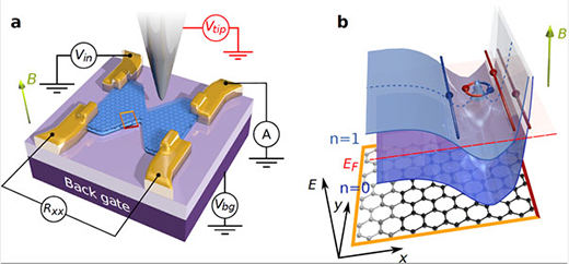 |
| a) Schematic of the studied sample. The graphene is protected by two layers of insulating hexagonal boron nitride (in blue) and a constriction shape has been defined. Four metalic contacts (in gold) are used to measure the device's resistance Rxx. A back gate allows to tune the graphene charge carriers density. Finally, a sharp metalic tip is biased by a voltage Vtip and is used to spot where the backscattering of charge carriers occurs in the quantum Hall regime. b) Schematic of the energy landscape at the sample edge (in the orange region in a, with border in red). At high magnetic field, the energy is quantized (blue layers that follow the potential landscape) and 1D edge channels appear where these levels cross the Fermi energy EF (electrochemical potenital). Here, counter-propagating edge channels flow along the same edge (blue and red) and an antidot (the loop) can appear between them, triggering charge carriers backscattering.
|
An enigma
|
|
The effect has several practical applications. It can be shown that the value of the electrical conductance or resistance in the quantum Hall effect is related to only two fundamental constants: the electron charge and Planck’s constant. Since it is the effect that allows the most accurate measurement of these constants, it has become a central part of the new international system of standards that came into effect in 2018, which is used to define the kilogram, volt, ampere, etc., among other things.
|
|
The quantum Hall effect is therefore used in all metrology laboratories, to calibrate a whole range of measuring devices. The fact that the quantum Hall effect can be observed at higher temperatures in graphene would allow the popularisation of quantum measurement standards, outside the framework of metrology laboratories, for example in industrial or university laboratories.
|
A bit of physics for a better understanding
|
|
Coming back to the physics of the phenomenon, an important point is that the charges accumulated on the edges of the sample in the quantum Hall effect are distributed on extremely thin “edge channels”, which are therefore “one-dimensional” but also “one-way”: all the electrons in the same edge channel propagate in the same direction.
|
|
The precision in the measurement of the fundamental constants is linked to the fact that the electric charges transported in these edge channels cannot undergo collisions, for “topological” reasons: to change direction, the charges would have to cross the inner part of the sample, but no energy level is available to accommodate them in this part, which is insulating.
|
|
Conclusion: it is impossible for them to undergo collisions and be sent back in the direction from which they come (backscattering). This “scatter-free” movement of electric charges is very attractive for a series of quantum electronic devices: the quantum states are protected by this mechanism, which can be exploited to imagine different concepts of quantum computers.
|
|
The fact that graphene shows very clear signatures of the quantum Hall effect at higher temperatures than any other material allows us to envisage a series of new applications in metrology and quantum computing.
|
|
However, some measurements performed on graphene samples in the last few years in several laboratories show that the “standard” model of the quantum Hall effect does not apply correctly in a large number of graphene samples.
|
|
For example, some measurements showed that the quantum Hall effect could be observed in graphene even though the inner part of the sample was conductive, contrary to the case of other materials. Without a detailed understanding of the phenomenon in graphene, robust applications cannot be conceived, thus it was necessary to solve the enigma posed by these intriguing observations.
|
A major step toward future applications
|
|
To achieve this, Nicolas Moreau, a PhD student in the UCLouvain laboratory of Benoit Hackens (IMCN/NAPS), relied on measurements performed with a unique “scanning gate microscope”, developed in the laboratory, on graphene samples fabricated in the laboratory of Christoph Stampfer (RWTH, Aachen). This microscope allows direct observation of the behaviour of electrons at a scale of a few nanometres.
|
|
The measurements surprisingly localised a large number of backscattering centres on the edges of the graphene samples. By combining the results with numerical simulations, the team was able to highlight the “Achilles heel” of the graphene quantum Hall effect: in most of the samples studied so far, the counter-propagating edge channels are not actually separated from each other by the sample’s “insulating” interior, but are very close to each other.
|
|
Hence electric charges can be backscattered if a localised impurity between the edge channels allows charge transfer between channels. Fortunately, these effects are governed by electrostatic phenomena that can be minimised by redesigning the devices.
|
|
This discovery, published in Nature Communications ("Upstream modes and antidots poison graphene quantum Hall effect"), is a major step forward in the understanding of the quantum Hall effect in graphene, towards the improvement of its measurement, and thus towards its application in metrology and quantum computing.
|

