| Aug 03, 2021 |
Development of ultra-high-resolution printed electronics using dual surface architectonics(Nanowerk News) National Institute for Materials Science, Japan (NIMS), has developed a dual surface architectonic process which enables to print submicrometer-scale circuit patterns by increasing the chemical polarity of predetermined areas on surface, thereby promoting selective adhesion of metallic nanoparticles to these areas (Small, "Dual Surface Architectonics for Directed Self-Assembly of Ultrahigh-resolution Electronics"). |
| In this process, the patterned polarity is achieved by simple treatments in ambient air which increase the surface’s adhesiveness to ink in the treated areas. As a result, very fine circuit lines (0.6 µm in width) can be printed. |
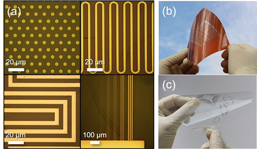 |
| (a) Microcircuit patterns printed using a dual surface architectonic process. Circuits printed on polyimide (b) and transparent (c) films. (Image: NIMS) |
| Printed electronics—electronic circuits printed using metallic and semiconducting inks—have been developed for a wide range of applications. However, the circuit traces printable using existing printing technologies, such as inkjet and screen printing, are too wide for certain applications. New technologies capable of printing finer circuit traces therefore had to be developed. |
| This research team recently developed a dual surface architectonic process which can be used to print submicrometer-scale wiring patterns by increasing the chemical polarity of predetermined microscopic areas of a substrate surface, thereby promoting selective adhesion of metallic nanoparticles to these areas. Simple photo and chemical treatments are applied to the substrate during this process. |
| First, preselected surface areas are activated by ultraviolet irradiation. A chemical treatment is then applied to these areas which increases chemical polarity and surface energy only in the UV-activated surface areas. Consequently, the surface’s adhesiveness to metallic ink increases precisely in the treated areas. |
| Because both treatments are simple and quick and can be performed in ambient air, use of the dual surface architectonic process is expected to significantly expedite and reduce the cost of printable electronic manufacturing processes compared to photolithography and other conventional printing methods. |
| Priways Co., Ltd. and C-INK Co., Ltd. have developed a metallic nanoparticle self-assembly system which can be used to print metallic nanoparticle inks at ultra-high resolution. The system will soon be put on sale along with primers specifically designed for use with it to enhance adhesion of metallic inks to different types of substrates. This research team will promote widespread use of this ultra-high-resolution printing technology for the production of printed electronics. |
| Source: National Institute for Materials Science, Japan |

