| Aug 03, 2021 |
Fabrication of printed high-performance thin-film transistors operable at one volt(Nanowerk News) National Institute for Materials Science, Japan (NIMS), has developed low-temperature-catalyzed, solution-processed SiO2 (LCSS), which subsequently enabled printing of high-performance thin-film transistors (TFTs) and three-dimensional circuits connecting various elements (Small Methods, "Layer-By-Layer Printing Strategy for High-Performance Flexible Electronic Devices with Low-Temperature Catalyzed Solution-Processed SiO2"). |
| These TFTs with an LCSS insulating layer, produced through printing alone, exhibited the highest field-effect mobilities among fully-printed TFTs ever recorded (70 cm2 V-1 s-1) at an operating voltage of 1 V or less. These results may facilitate the development of various printed devices, such as printed displays and highly sensitive sensors. |
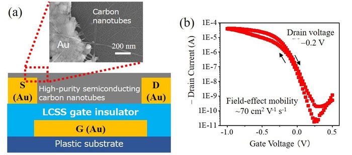 |
| (a) TFT equipped with an LCSS gate insulating layer fabricated solely by printing. (b) Electrical properties of the TFT. (Image: NIMS) (click on image to enlarge) |
| Printed electronics – electronic circuits printed using metallic and semiconducting inks – have been developed for a wide range of applications. Constructing practical electronic circuits through printing alone will require techniques for printing high-performance TFTs and three-dimensional circuits that connect all necessary electronic elements. However, fabricating TFTs and 3D circuits entirely by printing proved difficult, and previous printed circuit elements operated at low speed and required high operating voltages. |
| This research team recently developed LCSS, an interlayer insulating material for printed electronics, which can be formed through a low-temperature sintering process at 90 °C and processed into films. The use of this material enabled the fabrication of entirely printed high-performance TFTs and multilayer circuits. Printed multilayer circuits can be designed to increase electrical conductivity between layers through vias. |
| The TFTs constructed in this research exhibited one of the highest field-effect mobilities ever reported (70 cm2 V-1 s-1) at an operating voltage of 1 V or less. |
| Because LCSS layers can be formed on flexible, heat-susceptible materials, their application to the development of wearable devices is particularly promising. This research team will promote widespread use of this printing technique and insulating material for the production of printed electronics. |
| Source: National Institute for Materials Science, Japan |

